Introduction
The Nintendo DS is a wonderful gaming console. Its design completely revolutionized the way people imagined consoles when it released back in 2004. It introduced lots of new features such as a dual-screen, a touch input, wireless multiplayer and more. The architecture of the DS was considered really complex for its time. It features a dual-CPU, shared memory, retrocompatibility depending on the inserted cartridge, and more. The complexity of the console makes its boot process particularly intriguing from an embedded software perspective.
This article will explore in detail how the Nintendo DS boots, starting from a powered-off state to launching a game cartridge. Gaming itself will not be covered and the focus will rather be on technical details that allow the console to be alive. We’ll take a look at the hardware, follow the boot sequence chronologically, and explain how both CPUs coordinate and how the game cartridge is verified.
Prerequisites
Before going further into this article, you should make sure to be comfortable with a few concepts:
- Basic understanding of programming and computer science.
- Basic understanding of embedded systems concepts.
- Some knowledge of memory management, CPU registers, and bootloaders may be helpful for a deeper understanding.
- Some knowledge of assembly could be useful as well.
- Some familiarity with the ARM architecture is not necessary but will definitely be a plus.
Now let’s dive in the wonderful world of the Nintendo DS architecture and its boot process.
The Hardware Architecture Of The Nintendo DS
Understanding the hardware architecture of the Nintendo DS is essential to grasp the concepts that we will talk about later in this article. In particular, understanding how components interact with each other is important for later sections.
The Nintendo DS has a lot of different hardware parts, but we will only cover those that are essential to the boot process. It is composed of:
- Two interconnected CPUs
- Several memory regions
- Two cartridge slots which both play a specific role in how the console boots and starts games
Dual-CPU Architecture
The console is built around a dual-CPU design which consists of two ARM processors:
ARM7TDMI
You might be familiar with this CPU if you have some knowledge on the architecture of the Game Boy Advance. It is a 32-bit RISC CPU running at ~33 MHz[1], which is more than twice as fast as the GBA CPU, while keeping all of the original features. This is not the main CPU used by the console but rather a secondary CPU that is used to offload the main CPU from some of the charge of I/O operations. This is why it is placed right next to most of the I/O ports[2].
It is also used for audio processing, handling Wi-Fi and touch input, and for backward compatibility. When using it for the latter, its internal clock will run at 16 MHz like on the GBA[1]. That way, GBA games are still able to work perfectly fine.
ARM946E-S
This is the main CPU of the Nintendo DS. It is also a 32-bit RISC CPU but this one is running at ~66 MHz[1]. It features 12 KB of L1 cache, which is not present on the ARM7TDMI, 8 KB are used for instructions and the remaining 4 KB for data. Another of its perks is its 48 KB of Tightly-Coupled Memory (TCM) with 32 KB for instructions (ITCM) and 16 KB for data (DTCM)[2]. It is used for logic, 3D rendering, control flow, and handles most of the system’s execution.
However, because of a hardware bug in the ARM9, its real clock speed of 66 MHz can only be used with cache and TCM. The rest is limited to the 33 MHz bus clock. This glitch causes an additionnal 3 waitcycles in the CPU which drops its actual clock speed to ~8MHz which is even slower than the ARM7 from the GBA processor[1].
Memory Layout
The internal memory of the DS is mapped as followed[1]:
- 4 MB of main RAM (doubled in the debug version).
- 96 KB of WRAM (Work RAM) of which 64 KB (32-bit bus) are mapped to the ARM7TDMI and 32 KB (32-bit bus) are either mapped to the ARM7 or the ARM9 and used for sharing data between both CPUs[2].
- 60 KB of TCM (48 KB) and cache (12 KB) as mentionned above which are mapped to the ARM946E-S.
- 256 KB of firmware Flash.
- 36 KB of BIOS ROM with 4 KB mapped to the ARM9, 16 KB mapped to the ARM7, and 16 KB used for GBA mode when using retro-compatibility features.
Cartridge Slots
The Nintendo DS contains two types of cartridge slots:
- Slot-1: The main cartridge slot, used for DS games cards. It includes a secure area used for verification in the boot process and for anti-piracy checks.
- Slot-2: Intended for GBA cartridges. Like Slot-1, this slot is verified thoroughly.
When booting, the firmware checks the first slot (Slot-1) for a valid DS cartridge. If the cartridge is not valid or none is found, the firmware either launches the menu or checks the second slot (Slot-2) for a GBA cartridge depending on its configuration.
Note
More on that in the Game Cartridge Verification section.
Initial Firmware Boot
When the Nintendo DS is powered on, the control begins from an internal firmware which is stored in ROM. This initial phase is responsible for setting up the system to a known state, also responsible for running signature checks on inserted game cartridges, and preparing the hand-off to user software.
Power-On State
Upon power-up, the ARM946E-S CPU begins execution first while the
ARM7TDMI is held in a reset state and remains inactive during this phase.
The system starts executing from the BIOS, stored in the 4 KB ROM of the ARM9,
located at address 0xFFFF0000.
This effectively jumps to this assembly code[3]:
cmp lr, #0
moveq lr, #4
mov ip, #64, 12; 0x4000000
ldrb ip, [ip, #768]; 0x300
teq ip, #1
mrseq ip, CPSR
ipsip, orreq ip, ip, #192; 0xc0
msreq CPSR_fsxc, ip
ldreq sp, [pc, #448]; 0x000002f8
beq loc_000000d4
The purpose of this small code snippet is to protect against a stray reset vector that could be jumped to during gameplay. If that happens, this allows the system to enter a debug state rather than corrupting memory or crashing entirely. This protection logic is built into both ARM9 and ARM7 BIOS.
Note
If you want to read more details on how this piece of code really works, you can check out CorgiDS technical summary.
Once this protection is setup, the BIOS code has to run some other essential procedures[1]:
- Disabling interrupts.
- Setting up the stack pointer and initializing system registers.
- Clearing up WRAM, VRAM and part of ITCM to remove residual data and ensure predictable behaviour.
- Configuring the memory protection settings.
- Performing a checksum of the firmware, ensuring data integrity before proceeding.
ARM946E-S Configuration
After BIOS initial execution, the ARM9 continues to configure some critical low-level components. These steps are crucial for performance optimizations and setting up the communication with the ARM7.
The most important configuration the CPU does is setting up ITCM
(Instruction Tightly-Coupled Memory) and DTCM (Data Tightly-Coupled Memory)
memory regions. These are small memory regions of high-speed RAM placed
close to the CPU core[1].
As mentionned in an earlier section, the ARM9 suffers from a severe hardware
bug that greatly reduces its clock speed. However, the TCM and cache are the
only components that can be used by the intended 66 MHz clock of the
ARM9[3]. These are configured by the BIOS using the
CP15, which is a built-in system control coprocessor. This crucial step
allows a major performance improvement as TCM plays a role in how the
interrupts are handled[1].
Another configuration of the ARM9 is the initialization of the DMA (Direct Memory Access) controller. It ensures quick data transfer without using the CPU. During this step, the cartridge interface is also initialized, which allows both CPUs to communicate at a later stage with inserted games in either slot[2].
At this stage, the ARM9 is running in an isolated environment. The ARM7 is still inactive, and the system has not yet loaded or verified any game code.
Firmware Menu
Info
This stage is actually handled by the ARM7TDMI. We will talk about how it’s powered-on and synchronized with the ARM9 in the next section.
By default, the ARM7 will load the firmware menu from the SPI Flash memory, which is a small external chip located next to the CPU’s core memory. This firmware menu contains the home screen of the Nintendo DS like user settings, download play features, launch games, and more. The firmware can be configured to launch the game directly if a cartridge is inserted, therefore hiding the main menu[2].
The firmware is loaded into RAM and executed as any other software. It’s used as a lightweight operating system and takes over the boot process. If a cartridge is inserted and detected by the system, and the firmware has been configured to skip the main menu, then the cartridge verification will automatically begin, which we will cover in a later section[2].
Note
The cartridge verification usually happens before the firmware launches. However when configured to be skipped and upon successful verification, the game will launch directly.
How The Dual-CPUs Coordinate And Communicate?
After the ARM9 finished up all of its initializations and before loading the firmware, the ARM7 is completely dormant and held in a constant reset state. This part is really important because it explains how both CPUs are synchronized and how they communicate, and the dual-CPU architecture is one of the core features of the Nintendo DS.
Activating The ARM7
Once the ARM9 is initialized, it tries to activate and synchronize with the
ARM7. To achieve that, it sends a 4-bit value to the ARM7 on the IPCSYNC
register, telling the other CPU to wake up. Then the ARM9 waits in a loop for
a response from the ARM7. When it does, they both sync-up and run together as
one singular system[2].
The now awake ARM7 begins execution at 0x00000000 in its 16 KB BIOS ROM,
which is unlike the ARM9that starts at 0xFFFF0000. It handles a few important
things such as[3]:
- Setting up the RTC (Real Time Clock).
- Loading the firmware, which we covered in the previous section.
- Performing security checks on the game cartridge.
Being so close to I/O ports, the ARM7 is actually the only one able to access these regions. It also handles WiFi, touchscreen, and other features we won’t cover in the rest of this article.
Communication Between Both CPUs
With both CPUs online and synchronized, they need to communicate with each other. To do that, they use a dedicated IPC FIFO (Inter-Processor Communication FIFO) which consists of two 64 bytes queues with a maximum of 16 elements. Each element has a size of 32 bits. This works as an efficient bi-directional way of communicating different commands, small messages, or signals. There are two ways the other CPU can fetch the sent data, either through polling (resource expensive), or through interrupts[2].
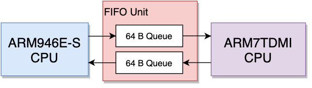 Copetti’s representation of the IPC FIFO[2]
Each message queue comes with a special 32-bit register called the IPC FIFO Control Register which holds a few status flags (full, empty, …) and some control bits (clear queue, enable interrupts when FIFO is either full or empty, …)[1].
The IPC FIFO is not the only way to communicate for the CPUs. They also have shared memory, a 32 KB region of the WRAM which is shared between the ARM9 and the ARM7. To avoid any issues, only one processor can access this memory at a time[1].
Game Cartridge Verification
Once the ARM9 and ARM7 are synchronized and working in harmony, the next step is for the ARM7 to verify the integrity and authenticity of the inserted game cartridge. This also enforces Nintendo’s anti-piracy and security mechanisms. Upon successful verification, the cartridge should correctly load the game data.
Note
The game cartridge verification only occurs on Slot-1, which corresponds to DS cartridges and not GBA cartridges. This is because only DS cartridges have a built-in signature and a secure area. Since GBA cartridges have no signature and therefore no verification at all, the DS simply boots into GBA mode and executes the card as a GBA would.
This is why we will mostly talk about DS cards in this section.
Why Cartridge Verification Is Necessary
Cartridge verification is crucial because it ensures that only Nintendo licensed games can run on the DS. This is especially important due to the early 2000s increase in piracy on earlier consoles.
Not only does this system prevent unlicensed games or malicious code from being executed by only allowing cartridges with a valid RSA signature in a dedicated secure area, it also avoid instability in the system. For example, if an official cartridge becomes corrupted of faulty in some way (bad headers, …), it could cause undefined behaviours or cause crashes within the system if executed without verification[2].
Structure Of A DS Cartridge
A cartridge contains a lot of information about its metadata and the game’s
program.
The first section in its memory is the 4 KB header, which contains
information such as[1]:
- Game title
- Gamecode (short code used to identify the game:
NTR-UTTDfor example) - Address of entrypoint
- Secure area checksum
- Nintendo Logo checksum
- Header checksum
After the header, there is the secure area, which contains sensitive boot
code and some signature data. It is 16 KB maximum in size ranging from
address 0x4000 to 0x7FFF. Its size depends on the source address of the
ARM9 boot code ROM. On some cartridges, the source address might be after the
allocated range (src >= 0x8000) and therefore won’t have a secure
area[1].
The next area contains the main code for the game and all its assets. Its size is variable but the overall size of the cartridge cannot go over 512 MB.
Loading The Cartridge And Verification Process
Since DS cartridges are not memory-mapped, in order to be loaded in the
console, they must be loaded into RAM at address
0x27FFE00[1][2].
To achieve that, the DS sends an 8 bytes command and waits for a 4 bytes
response from the cartridge. It will then load more data from the cartridge
until it is fully loaded within RAM[3].
Note
GBA cartridges on the other hand are memory-mapped and directly loaded into the ARM7’s WRAM.
When reaching the secure area of the loading process, some verifications need
to be done. Nintendo uses a symmetric encryption system based on the
Blowfish algorithm for the first 2 KB of the secure area and for the
communication between memory and the Slot-1 interface. This algorithm generates
two keys, KEY1 which is obtained by using the gamecode (cf. last
subsection), and KEY2 which is obtained by combining the internal clock (RTC)
and some other values from the header[2].
First, the ARM7 retrieves the chip ID of the cartridge and stores it in
RAM. The first 8 bytes of the encrypted region of the secure area contain a
specific string called the secure area ID. This ID has to be decrypted to
encryObj, otherwise the entire 2 KB is overwritten with random bytes
preventing the game from being loaded. If the string is correctly decrypted,
it is replaced with another word to protect the
algorithm[3].
Then the chip ID is retrieved multiple times randomly, and must match exactly
the chip ID retrieved earlier.
After all the verifications succeeded, the rest of the secure area is loaded
in random order of 4 differents 2 KB blocks and reconstructed in RAM. Only
then will the firmware be
executed[2][3].
What happens if the verification fails or if no cartridge is inserted?
If this happens, the system will simply execute the firmware and not show any bootable games in the menu. However, if a GBA cartridge is inserted, then this won’t cause any issue and the user will still be able to boot into it.
Conclusion
The Nintendo DS boot process is a fascinating example of how complex systems can be orchestrated through careful coordination. From the moment power is applied, the ARM9 takes control, initializing memory and setting up the system environment before waking up the ARM7 and synchronizing with it. Only then does the game cartridges are verified and the firmware is loaded, among other things handled by the ARM7 that we didn’t cover.
What makes the DS especially interesting is its dual-CPU architecture. It’s a relatively rare setup in handheld consoles of its time. This design allows a clear separation of responsibilities between game logic and hardware access, but it also introduces complexity in terms of memory sharing, synchronization, and communication. The use of shared WRAM, IPC FIFO, and interrupts demonstrates how low-level systems must be precisely engineered to avoid conflicts and maintain performance.
Understanding this boot process isn’t just about retro curiosity, it also sheds light on the kinds of problems embedded systems engineers face every day. These principles remain as relevant today as they were in the DS era.
If you want to learn more on this subject, feel free to read the articles linked in the bibliography.
Bibliography
[1] GBATEK - GBA/NDS Technical Info:
https://problemkaputt.de/gbatek.htm#ndsreference
[2] Nintendo DS Architecture | A Practical Analysis by Rodrigo Copetti:
https://www.copetti.org/writings/consoles/nintendo-ds/
[3] Booting the Nintendo DS – a technical summary – CorgiDS:
https://corgids.wordpress.com/2017/07/28/booting-the-nintendo-ds-a-technical-summary/