Introduction
Before diving into this article, a basic familiarity with CPU architecture and terminology—such as SDRAM, cores, cache, and clock speed is assumed. Additionally, readers should have some awareness of common GPU applications, whether in video games, machine learning, or cryptocurrency mining.
While the terms “GPU” and “Graphics Card” are often used interchangeably, a GPU (Graphics Processing Unit) is not the same as a graphics card. The GPU is just one component of the graphics card, which also includes heat sinks for thermal management, voltage regulators to ensure stable power delivery, PCIe interface for communication with the motherboard or video outputs (e.g., HDMI, DisplayPort). The only non-GPU component we’ll discuss in detail is SDRAM (Synchronous Dynamic RAM), as it plays a critical role in the GPU’s memory hierarchy and performance.
At its heart, a GPU is optimized for parallel processing—performing the same operation on large datasets simultaneously. A modern high-end GPU1 from 2024 typically contains thousands of processing cores, while a CPU2 from the same year usually features between 8 and 64 cores. These GPU cores operate at clock speeds approximately 1.5 to 2 times slower than contemporary CPUs. However, the GPU’s massively parallel architecture enables it to process significantly more data per clock cycle. This fundamental difference is why GPUs are essential for parallel workloads such as 3D rendering, artificial intelligence training, and large-scale scientific computations.
The following sections will first examine the hardware components that enable this parallel processing capability before discussing their implications for software performance and limitations. Please note that this article mainly focuses on Nvidia hardware even though similarities exist with AMD and Intel GPUs.
Block-Based Parallelism
The Hardware Hierarchy
The GPU is divided into several parts. Among them, the processing core is taking the vast majority of the space on the chip.
As GPU leverage its true power by parallelizing tasks, it needs a hardware that fits this hierarchy. But simply taking CPU cores and putting them together is not a solution as this kind of core is not properly suited for embarrassingly parallel tasks because of its complex instruction set that provides much more flexibility. Instead, the GPU is organised under a hardware hierarchy where every components aims to balance the workload efficiently inside of its sub-units.
The processing core itself consists of several independent units called Graphics Processing Clusters (GPCs). One of the key advantages of this design is scalability—for instance, the AD102 (used in the RTX 4090) incorporates 12 GPCs, while the smaller AD104 (found in the RTX 4070 Ti) uses just 5.
Each GPC is made of several Streaming Multiprocessor (SM). To understand SMs, we must first introduce an abstract concept: the Warp. Whenever a program on a computer is running, it relies on the registers stored in the processor that is applying the operations to execute the sequence of instructions. In other words, a program is nothing more than some data and some instruction put together. In SM, a Warp is the logical definition of the data part of this model. However, a warp does not hold the data for a single execution of the “program” (ie. the sequence of instructions), but for dozens of simultaneous executions on different copies of the data. In summary, if a given “program” requires a specific amount of data for execution, the Warp represents that data duplicated multiple times. Each of these duplicated instances is called an “execution thread” (or just “thread” in short), which is a logical notion analogous to CPU threading.
In term of hardware, a standard SM contains:
-
Register Files: This unit holds the registers that are making up each of the warps. The register file is split into 32-bit registers that can be dynamically reallocated between different data types, like 32-bit integers, 64 bit floating point numbers, and (pairs of) 16 bit floating point numbers. The amount of registers used will vary throughout time during execution of the different “programs” attached to each warp.
-
Execution Units: This unit aims to compute and is similar to an Arithmetic and Logic Unit (ALU) in a CPU. These units can take the shape of floating point units, integer units or even more specialized units such as ray-tracing units or tensor units. Most of these units can process multiple threads simultaneously, sometimes even an entire warp at once.
-
Cache: This unit represents all of the memory space available to every execution units. This article will not explain in detail as we will come back to this later on.
-
A Scheduler: This unit is responsible for deciding which warp among those currently in the register files will be processed by the execution units. This scheduler therefore masks some delays by switching to another warp which has its next instruction’s operand available. Please note that, unlike CPU, there is no speculative execution or instruction pointer prediction.
This list is non-exhaustive but is a solid base to begin with. To give you an idea of the scale in this hardware hierarchy, the GPU GA1023 holds 7 GPC each containing 12 SMs with 1 ray-tracing core, 4 tensor cores and 128 CUDA Cores. Please note that the term “CUDA Core” is slightly misleading: in different Streaming Multiprocessor architectures, CUDA Cores can consist of different units (32-bit integer and 32/64 bit floating point units)4.
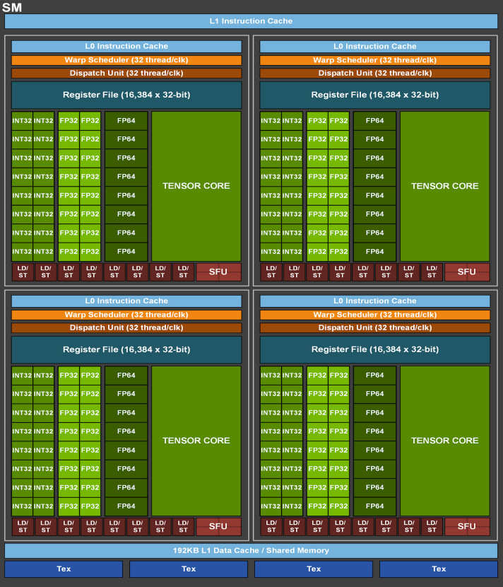 An overview of the GA100 Streaming Multiprocessor taken from this nvidia publication5
What is SIMD?
One of the key concept behind those Warps holding threads all running the same sequence of instruction is a principle called “Single Instruction Multiple Data (SIMD)”. Usually, this hardware concepts are hidden behind software API. Luckily for us, all of these APIs mostly agree on some key principles when it comes to abstracting the hardware for a more “developer-friendly” use.
When it comes to code, the “program” executed onto a GPU is called a kernel. The kernel is merely a sequence of instructions that aims to be executed concurrently (their execution order is non-deterministic) and in parallel (they occur simultaneously on different execution units). These kernels are dispatched onto the different SMs available on the GPU.
In order for the developer to have the hand on how all of this threads are dispatched, the API creates a basic unit called a Block. A Block represents an arbitrary amount of threads that will be inserted into the warps of an SM. If the number is not round, some threads in the warp are simply not used. A good practice is therefore to stick to a multiple of the number of threads present in a warp in order to achieve the best performance and fill our warps as much as we can. Please note that the block value has to be less than or equal to the maximum value of thread that a single SM can hold. Blocks are then stacked into a 1, 2, or 3 dimensional grid. This is called the Block Grid6. The kernel is then launched on this block grid and executed in every single thread context.
However, in order to feed the GPU with data, there is no real “common way” of doing it and the methods will highly depend on the software you’re using.
Now that we have both a kernel and some data, we can leverage the full power of our GPU! Can’t we?
Memory Hierarchy
Types of memory
A kernel is not only about loading and storing data, it’s also about efficiently managing where that data is stored. In this context, GPU includes several kind of memory:
Private Memory (Register File)
The fastest memory available to each thread, residing directly in the Streaming Multiprocessor’s (SM) register file. Each thread has exclusive access to its own registers, enabling zero-latency access to frequently used variables. With typical GPUs offering 255 registers per thread, this memory is precious and extremely fast - operations can complete in a single clock cycle. The compiler aggressively optimizes to keep variables in registers whenever possible.
Local Memory
A thread-private memory space that serves as overflow when registers are exhausted or for variables that cannot fit in registers (like large arrays or structures). Despite being logically “local”, it physically resides in global memory and is cached in L1/L2. Access latency is significantly higher than registers (100+ cycles), making excessive use detrimental to performance. The compiler automatically spills registers to local memory when register pressure becomes too high.
Shared Memory
Shared Memory is located in each of the SM units. This holds a few hundreds Kilobytes of data maximum. This data is therefore shared across all threads of a specific thread block, enabling efficient inter-thread communication. Shared memory operates at near-register speed because it’s implemented as on-chip SRAM.
Global Memory
Global memory holds several Gigabytes of data and is stored in the SDRAM mentioned earlier that is placed onto the graphic card, right next to the GPU. It is the only instance of memory that is not strictly located inside of the GPU but it acts as a buffer between the CPU and the GPU for the massive amount of data the GPU consumes. The bandwidth between this memory and the GPU can reach more than a Terabyte per second (e.g. 3.35TB/s on NVIDIA H100 SXM7). In comparison, the bandwidth between the CPU and the RAM is tens of Gigabytes per second. Despite its large capacity, global memory suffers from high latency, requiring careful access patterns for optimal performance.
L1 and L2 Caches
Each SM contains a dedicated L1 cache that buffers frequently accessed data from global memory. It typically holds a couple hundred of Kilobytes per SM. CPUs also maintain an L1 cache but it is fully hardware-managed. In GPUs that cache is mostly programmer-managed. The programmer must explicitly move data into the cache (e.g., using shared in CUDA) and manage how it is used.
L2 cache is a unified cache shared across all SMs on the GPU, typically several megabytes in size. The L2 cache acts as a middle layer between the SMs’ L1 caches and global memory, helping to reduce pressure on the memory controllers. While slower than L1, the L2 cache is significantly faster than accessing global memory (DRAM) and plays a crucial role in improving memory bandwidth and latency.
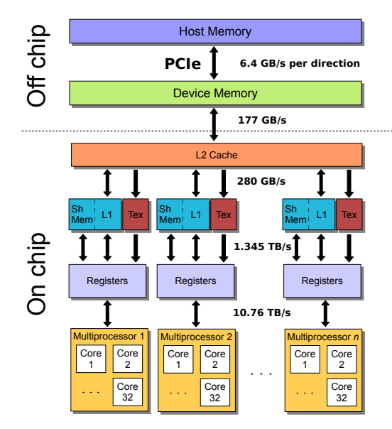
A schematic of the memory hierarchy of the Nvidia Fermi architecture with the peak bandwidth between each layer taken from this article8. All numbers quoted correspond to the aggregate bi-directional rate, with the exception of the PCIe rate which is per direction.
Abstraction and Control
While many memory optimizations are handled automatically (such as caching and register allocation), programmers can further optimize performance through specific APIs and abstractions:
- CUDA and HIP provide direct control over memory placement using keywords like shared for shared memory or global for device memory. These require manual data movement between memory tiers but enable precise optimizations, such as staging global memory data into shared memory for block-wide reuse.
- Frameworks like Kokkos abstract memory spaces (e.g., scratch_memory_space), allowing developers to target optimal memory tiers (like shared memory for scratchpad data) without architecture-specific code.
I have my GPU, my instructions and a correct memory layout, nothing could go wrong now, right?
Synchronization (Barriers)
I am sorry to deceive you, but we are missing an essential element in massively parallel execution: synchronization.
First, it is important to keep in mind that the GPU is an external device and is therefore not synchronized with the CPU. The two devices communicate through PCIe port9. Therefore, the CPU is responsible for sending the kernel code as well as the data that will be processed by the block grid but has no clue about the advancement of the operations after that.
Next to the processing core that we find on the GPU, we can find the Gigathread engine. Its main role is to dispatch blocks onto SMs and follow the state of the overall GPU task. Kokkos for example, proposes a fence10 implementation that blocks the CPU program until all operations on GPU are marked completed. Similarly, CUDA API provides developers with cudaDeviceSynchronize.
When executing a kernel, threads within the same warp (a group of 32 threads in modern GPUs) follow the same program counter (PC). However, if threads diverge—for example, due to an if statement—the warp scheduler masks inactive threads, allowing the warp to continue executing only the active paths. While this preserves correctness, it reduces parallel efficiency since divergent threads serialize execution. To coordinate threads, GPUs provide barrier instructions, which force all threads in a block to reach the same point before proceeding. Barriers are essential when threads share data (e.g., via shared memory) and must ensure all writes are visible before others read them.
Different frameworks expose barriers with similar semantics:
- CUDA:
__syncthreads() - OpenCL:
barrier(CLK_LOCAL_MEM_FENCE) - Kokkos:
team_barrier()
Please note that OpenCL barrier(CLK_GLOBAL_MEM_FENCE) instruction synchronizes all SMs by splitting work into dependent launches. This ensures that all threads have finished the current phase of the kernel. It is easy to see that this method is not very effective as it freezes all of the SMs while waiting for every others to complete.
Conclusion
Understanding the architecture and principles behind GPUs provides a solid foundation for exploiting their computational power. Whether you’re rendering complex 3D scenes, training machine learning models, or accelerating scientific simulations, GPUs offer unparalleled performance.
However, theoretical knowledge alone isn’t enough. To truly leverage GPUs, diving into practical implementations is essential. APIs like Vulkan, OpenCL, CUDA, and frameworks like Kokkos provide the tools to translate these concepts into real-world applications. A great starting point is the “Hello World” of GPU computing: a simple square matrix multiplication. This exercise introduces key concepts like kernel dispatch, memory management, and thread synchronization—all while demonstrating the dramatic speedups GPUs can achieve over CPUs.
So, take the next step: pick an API, write your first kernel, and experience firsthand how GPUs unlock new possibilities in computing. The revolution in parallel computing is yours to harness.