Table of Content
Introduction
One of the biggest challenges of the last decades was to manage more memory, with ever-faster access. Over the years, we have subdivided memory in multiple parts: hard drive, CPU’s caches, RAM, all to meet the inflection point between efficiency, space, and cost.
One type of memory is RAM.
RAM, which stands for Random Access Memory, is a form of memory that can be read or written in almost the same amount of time irrespective of the physical location of data inside the memory, hence the term Random Access.
DRAM, for Dynamic RAM, is a type of RAM that stores each bit of data in a memory cell by storing electric charges in capacitors.
We do not use RAM to save data in the long term, but to have fast access to it. This
article concentrates on DRAM. We will walk through its inner workings and its
optimizations, from transistors to chips and briefly covering iMC commands.
We will also focus on the refresh process, the reasons behind it, and how much time it really consumes.
This article will not talk much about CPU’s communication to the DRAM.
DRAM’s architecture
One Memory Cell
To understand the overall workings of DRAM, we need to comprehend its inner workings.
At the most basic level, DRAM is made of memory cells.
A memory cell is composed of two elements:
- a capacitor
- a MOSFET transistor
Gthe gateDthe drainSthe source
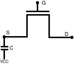
The MOSFET is used as a gate, by activating or deactivating G (image
above), to allow electricity to flow from D to S to charge the capacitor C.
To discharge the capacitor, we can use the same process with the MOSFET
to allow electricity to flow in the opposite direction (S to D), enabling
charges to escape the capacitor, emptying it.
The last two sentences explain the fundamentals of DRAM.
When a capacitor is discharged (0 V), we consider that the memory cell
stores a 0. Similarly, when a capacitor is charged (1 V), we consider the
cell stores a 1.
Thus, with one capacitor and one MOSFET we are able to store one bit.
One Bank
Now that we are able to store one bit, we would like to store thousands.
Memory cells are organized in a matrix, called a bank:
- each
MOSFET’s drain in each column is connected together by a wire. These columns are called bitlines. - each
MOSFET’s gate is connected to the others within each row. These wires are called wordlines.
Organizing memory cells in a matrix enables us to find any bit, or any cell, by intersecting two wires, its bitline and wordline. This intersection is the address of the bit.
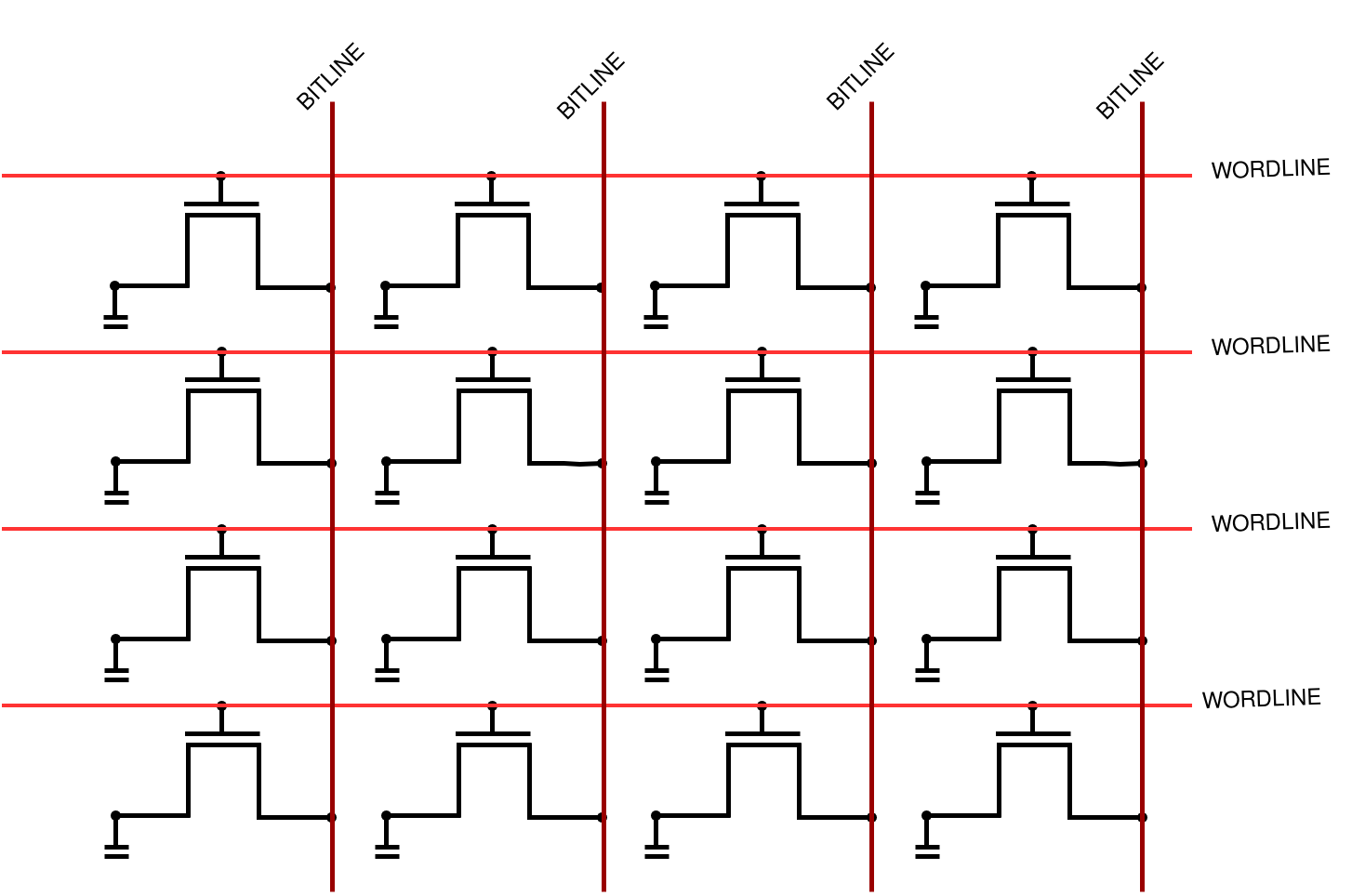
When we activate a wordline, we “open” the gate, allowing electricity to flow from all the capacitors on this wordline to their corresponding bitlines (and vice-versa). Then, we select the desired bitline to read, or write a value to.
These bitlines and wordlines are connected together to their respective decoder. Thus the wordline decoder can address its 4 wires using 2 bits.
If it were not for the row/column organization and each cell had its own wires, we would have 32 wires as we need one for the gate and one for the
MOSFET, eight times the wires needed by the matrix ! Minimizing wires is very important in electronics as it prevents space use and overheating.
Within a bank, we group bitlines in columns. The column’s width can either be
4, 8 or 16 bits (thus a column contains 4, 8 or 16 bitlines). So, in
reality we are not selecting a specific bit, or memory cell, with its
wordline and bitline. We are selecting a group of bitlines (let’s say 8)
from a specific column and wordline.
Manipulating a group of bitlines instead of one by one allows for more efficiency when reading: we fetch/read data by group instead of bit per bit. A column width of 8 is more common, as it enables us to directly manipulate bytes. Manipulating groups instead of individual bitlines requires also less addressing bits: we only need to select the column, not the bitlines.
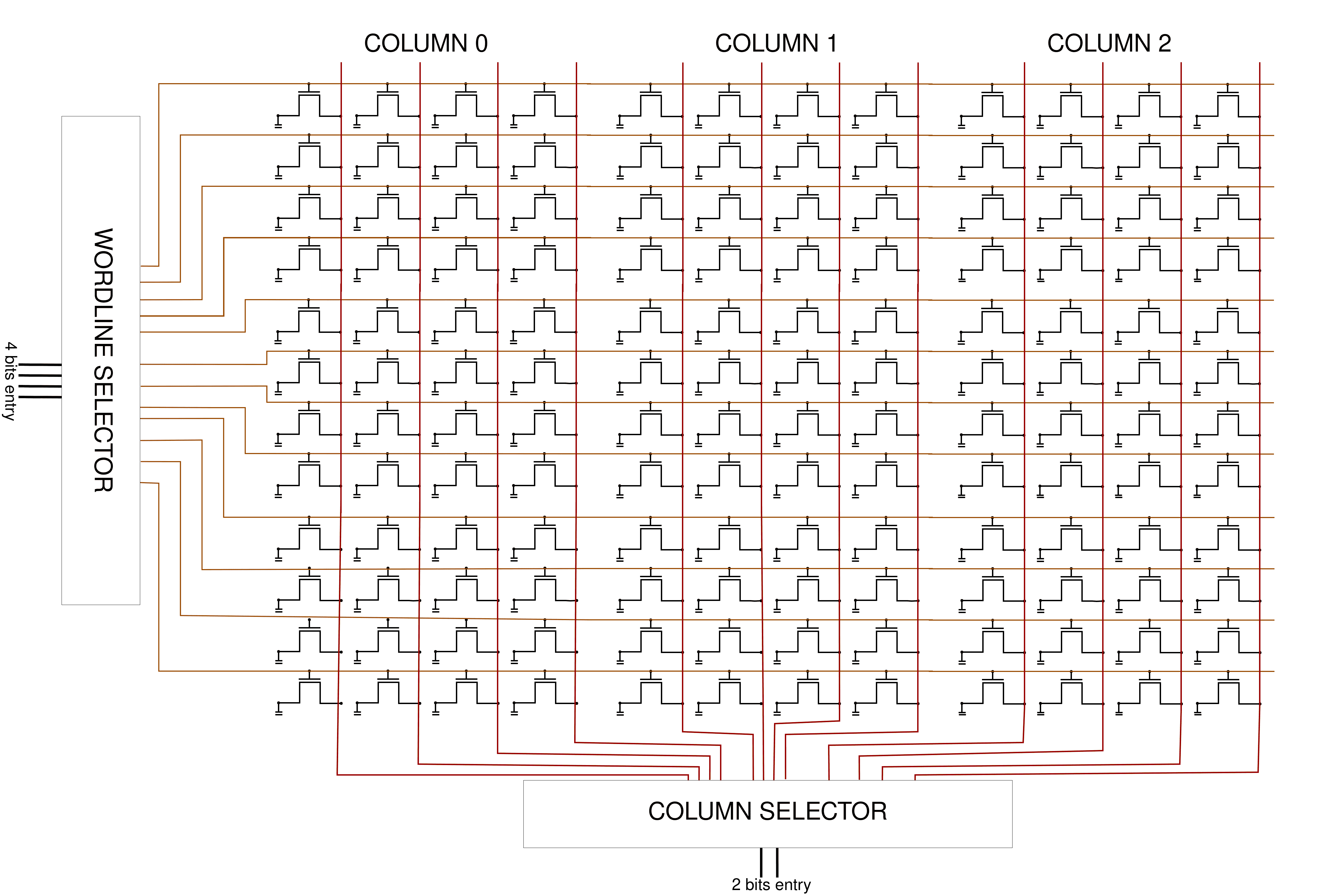
The schema illustrates the addressing of a 12 wordlines x 12 bitlines bank, with bitlines grouped by
4. We only need4-bitaddressing for the 12 wordlines and2-bitaddressing for the 3 columns. Please note this schema only illustrates bank addressing (not reading and writing).
One chip (or memory die depending on sources)
One chip contains several banks. Each bank can work independently and in parallel with the others, but within each bank, memory access is serialized.
The number of banks by chip is decided by the JEDEC standard for that
generation. Thus,
- for DDR3, we have
8banks per chip, - for DDR4,
16banks per chip (4bank groups of4banks) - for DDR5,
32banks per chip (8bank groups of4banks)
Since DDR4, banks are organized in bank group within a chip to increase performance. We will abstract this.
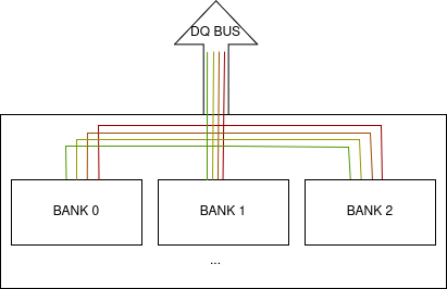
The chip is communicating with its banks through a memory data bus named DQ.
The width of this DQ data bus is the same as the bank column’s width.
Indeed, each bitline of the selected column is connected at one of the DQ
bus’s pin.
One rank
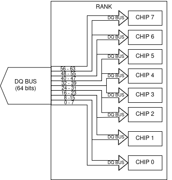
One rank contains multiple DRAM chips. A rank communicates with the CPU through a data bus.
For the sake of calculation, we will assume that this data bus is a
64-bitdata bus ofDDR3generation and8chips per rank.
If this bus’s width is 64 bits, then the rank outputs 64 data bits at
once by outputting 8 bits from each of its 8 chips in parallel.
Let’s dive deeper into the relationship between the data bus width and the column width of each chip’s bank :
- With a
64-bitdata bus, we have a64 / 8 = 8bitsDQbus. So, the column’s width is also8bits (bitlines). - But with a
32-bitdata bus, we have32 / 8 = 4bitsDQdata bus and for a128-bitdata bus, we thus have a16-bitDQdata bus.
In reality, the rank bus and the chip
DQbus are the same. Indeed the rank’s64-bitDQbus is split between the chips’8-bit buses. For instance:
chip1will have the pins0to7of theDQbuschip2will have the pins8to15- … allowing parallelization within the bus.
One DRAM
A DRAM is also composed of multiple channels. Each channel is an
independent wire that connects multiple ranks to an iMC (CPU memory
processor).
These channels allow true parallelism between groups of ranks.
Technically, each channel connects to one
DIMMmodule, and each module contains one or more ranks. But, DIMMs usually have one rank, except dual-rank or quad-rank DIMMs.
When the CPU decides to read information from the DRAM, it
uses the desired physical address to select the correct iMC (CPU side).
The selected iMC activates the desired rank of the DRAM by its
channel through the DRAM’s CS_n pin.
For this example, we will use a DDR3 with a 32-bit DQ bus, 2Gb x8 components.
You can find its pinout specification here.
This DDR3 thus has:
- 4 chips (x8 components, thus 32 / 8) per rank.
- 8 banks per chip (JEDEC standard).
- each bank’s column has a width of
8bitlines (the x8).
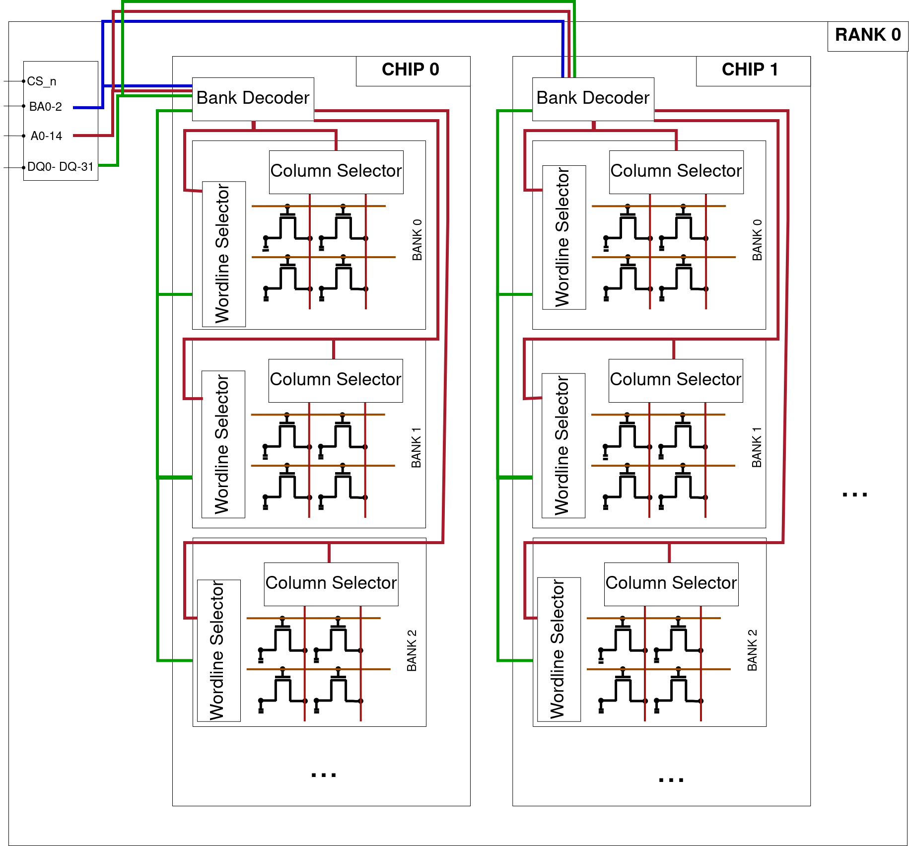
For simplicity, only two bitlines, wordlines, chips and 6 banks are shown.
- First, the iMC can select the correct rank by activating CS_n of this rank.
- We can then specify to the decoder the desired bank through the
BA0toBA2pin. - The decoder can activate the correct wordline address of the previously
selected bank with
A0-14pins. - Once the wordline is activated, it can specify the column (group of
bitlines) address through the same
A0-A9pins. - Then we can use the DQ bus to read and write data.
For instance, let’s say we have written “Hello World” and want to read it. Each letter is contained in the same bank, in the same row/column address of each chip. Thus, we specify the desired bank, wordline, column, and then we fetch a byte from each chip :
          Chip0  Chip1  Chip2  Chip3
beat 0:     H      e      l      l
beat 1:     o     ' '     W      o
beat 2:     r      l      d      !
We actually need three readings, called beats, to get the full message.
How do we RAMember
Reading and writing
Now that we understand the organization within the DRAM, let’s look
into the process of reading and writing.
As seen before, the CPU interacts with the DRAM through pins. But the information given through them needs to be decoded with selector circuits.
So, to select the correct wordline, we use a decoder that, with the given address, activates the correct row (of the correct bank of the correct chip …).
For the bitline, we need more than a decoder. Indeed, we need to select from which bitline we will read and return its data. A multiplexer seems the best choice, but in the case of writing, we cannot “give” to the multiplexer the data to write.
Thus, for the bitlines, a MUX-DEMUX, multiplexer and demultiplexer
combined, is used. This way, the CPU can decide whether it wants to read,
and activate the MUX-DEMUX as a multiplexer, or write,
and use it as a demultiplexer.
So, with the activated wordline, we can open the “gate” of memory cells to allow electricity to flow:
- from the activated bitlines to their capacitors to write
1or0 - from the capacitors to their bitlines to read the value
But how do we decide to read or write ?
Two other pins are used on top of A0-14, B0-2, CS_n, DQ:
RASandCAS, to activate wordlines or bitlines. They are active low.WE, to write if active (otherwiseread).
The protocol of reading and writing requires a strict sequence:
- First, we activate
RASto select the correct wordline with the given address. - Then,
CASis activated to select the correct bitlines with the newly given address.- If the
WEsignal is triggered, theMUX/DEMUXis used as demultiplexer to write the data contained in the DQ Bus. - If it is not active, the data contained in the memory cells will be read and
written onto the
DQ Bus.
- If the
A Self Destructive Reading
When we explain how capacitors are used to store data, we did not explain how the reading was done.
In order to read from a capacitor, we need to open the gate of the memory cell to check if electricity flows from the capacitor. But doing this empties the capacitor of its charges, if any, making reading a self-destructive operation because reading a value from a capacitor involves discharging it.
Furthermore, when we activate one wordline, we open the gates of all memory cells of that wordline. This means that we let electricity flow from all the capacitors of the wordline to the bitline, discharging an entire row.
So, we need to be able to restore the values of entire rows each time we read from them.
For this, we precharge the bitlines: if 0V means 0 and 1V means
1, we precharge the bitline 0.5V. If the capacitor is charged, the bitline
voltage will go up, as electricity goes from the capacitor to the
bitline. Whereas if the capacitor is discharged, it will gain charges from
the bitline : making the bitline’s voltage go down.
The precharged bitlines allow us to double the difference between charged and empty capacitors as the range becomes
[0.5 - d, 0.5 + d]compared to[0, d](withdbeing the delta difference added or taken by the capacitor) if not precharged.
We now need to detect the bitline charge level, to mark the memory cell as 1
if the bitline voltage is greater than 0.5V or 0 if less than 0.5V.
For this we use sense amplifiers.
The sense amplifier compares two voltages: the voltage from the wanted
bitline and the voltage with a reference precharged bitline. It uses the
voltage difference between the two to determine, using transistors, a 0 or a 1.
This circuit is also used as a latch, meaning saving the read value in an
infinite loop.
Do not forget that we activate an entire wordline, so the sense amplifiers
save values for the entire row, and give them as inputs to the MUX-DEMUX.
The MUX DEMUX can then decide by reading the column’s address, which ones it
needs.
This part is important: by first selecting the row, then reading and saving all its values, then selecting the correct one, we justify the shared
A0-A14address bus: we are never using both addressing at the same time, always rows first, then column.
Furthermore, as the sense amplifier is also used as a latch for an entire row, if we want to read the same row multiple times, we do not have to actually read the value from the capacitors, only the values in the sense amplifier latch!
A single sense amplifier keeps its data in a
6-transistorloop. Compared to amemory cell, one latch takes a lot of space. So, in reality, memory cells are not organized in a perfectly square matrix. We tend to put as many memory cells connected to the same sense amplifier, to make the bitlines longer and wordlines smaller!
To conclude, once we have read the value, we can now restore the used capacitors, by forcing the bitline voltage to the value contained in the sense amplifiers.
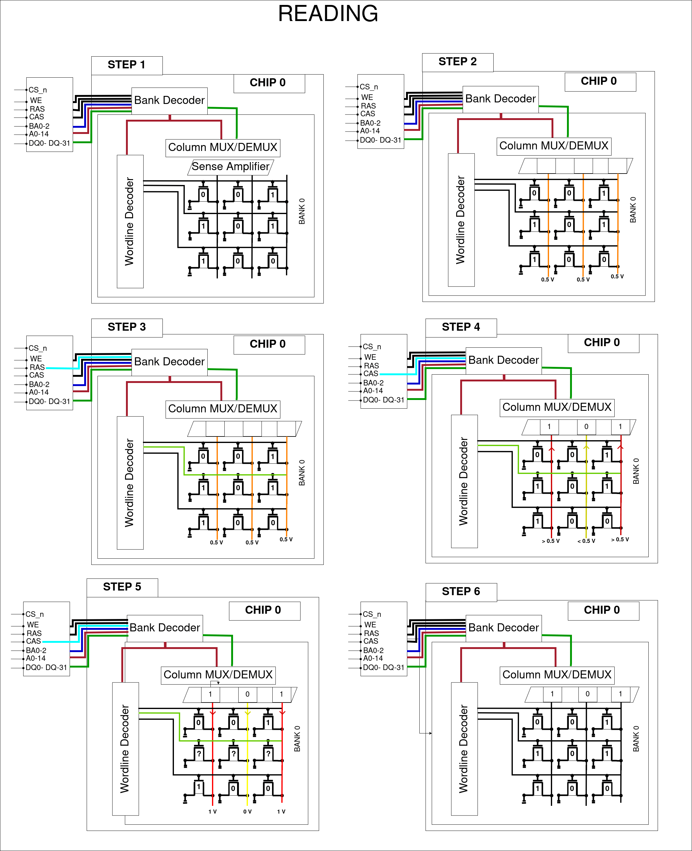
To summarize:
- STEP 1 : Nothing happens yet
- STEP 2 : We precharge the bitlines
- STEP 3 : We select the correct wordline
- STEP 4 : Depending on whether the capacitor is charged, the bitline
voltage will drop below
0.5Vor rise above. The latch detects the change and memorizes the corresponding value. - STEP 5 : By activating the wordline, the charges contained in the
capacitor change. We no longer have
0or1, but something in between. We restore their values from the sense amplifier. - STEP 6 : Back to step 1, but the values are still kept in the sense amplifier
For writing, we actually use the same process :
- Precharging the bitlines
- Selecting the wordline
- Then we change the value of the sense amplifier latch of the wanted index to its new value from the DQ Bus.
- Thus the capacitor is automatically updated when it is refreshed with the value contained in the sense amplifier’s latch.
Refresh rate
But reading and writing are not the only issues with DRAM, a capacitor will, by
itself, lose charge, leak, over time, meaning every 1 in the memory will
turn to 0 with a given period of time.
This leak issue has favored the use of MOSFET. Bipolar transistors need constant power to their gates : it consumes more power and lets charges leak faster from the capacitor. As MOSFETs have their gates isolated by a Metal-Oxide-Semiconductor layer, when they are off, few charges can escape.
First, let’s see how much longer can a capacitor save information. DRAM
capacitors are built-in stack capacitors. The exact time for a capacitor to
hold a charge depends on the sources, the DRAM used, the temperature and the
experiment done (cf. ref,
ref).
But, the JEDEC standard assumes a DRAM’s capacitor must retain a charge for
at least 64 ms.
This means we need to refresh this memory every 64 ms to be sure no
capacitor loses its charge.
Some researchers have succeeded to perform a retention time of 4096 seconds on an
8 Gb DDR3. You can find the research paper in the following link.
We actually already refreshed before: when we read or write, we update the content of the capacitors of an entire row with the value contained in the sense amplifier’s latch.
So, refresh just means reading the value of a row. These values are saved in the sense amplifier and we write those values back in the capacitors.
But, we still need to refresh the entire memory, row after row, every
64 ms !
How much does it cost - Time VS Space
First, let’s comprehend how CPU commands work.
The memory controller (iMC) that interfaces with DRAM uses a series of
commands sent through specific pins.
There are five major commands that are used to access DRAM (via timing
combinations of RAS, CAS, WE):
PRE: to precharge the bitlineACT: to activate a wordlineWR: to writeRD: to readREF: to refresh
The refresh (REF) command ensures that every DRAM cell is refreshed once at
a x refresh window. A DRAM chip refreshes several rows when receiving a single
REF command, which takes tRFC time to complete.
If the
REFcommands only refresh one row at a time, we call ittRFC1. If it refreshes two rows at a time,tRFC2… tRFC2 and tRFC3 only exist since DDR4.
So, how much time does a REF command take ?
We could argue a REF command is just a combination of multiple PRE + ACT
commands done on each row. But in reality, tRFC refreshes multiple wordlines
at once in a single REF command. tRFC also depends slightly on the bitlines'
length: the longer the length, the more time a sense amplifier detects a change.
We also have to take into account that banks can refresh their rows in parallel
because they have an independent wordline decoder. To make sure we start our
analysis from the right refresh time, we can directly look in DDR’s datasheet.
We will take, for example, a DDR4 3200 U-DIMM, we can find in its documentation
the required time for a full refresh.
| DRAM Size | Refresh Mode | Minimum time Required for a full Refresh |
|---|---|---|
| 4 Gb | tRFC1 | 260 ns |
| 4 Gb | tRFC2 | 160 ns |
| 4 Gb | tRFC4 | 110 ns |
| 8 Gb | tRFC1 | 350 ns |
| 8 Gb | tRFC2 | 260 ns |
| 8 Gb | tRFC4 | 260 ns |
| 16 Gb | tRFC1 | 550 ns |
| 16 Gb | tRFC2 | 350 ns |
| 16 Gb | tRFC4 | 260 ns |
The value in the table above can be reinforced by 4 Gb DDR3,
where we see that tRFC also takes 260 ns (similarly to 4 Gb DDR4 tRFC1)
As we can see, we are well below 64 ms: an entire refresh, even one row
at a time, of a 16 Gb DRAM takes less than 1 ms.
Logically, for the DRAM to become unusable because of its refresh would
need a tRFC of 64 000 000 ns. By making the approximation that the time needed
is proportional, since a 4 Gb DRAM requires approximately 100 ns, then, in order to reach
a 64 000 000 ns refresh time with tRFC1, 984 615 Gb would be the theoretical limit.
So, the DRAM can handle a size of 1 TB without problem !
Of course, the inflection point of usability is well below 984 615 Gb, as the DRAM will probably become too slow if the refresh time takes more than a third of the
64 msrefresh cycle.
Conclusion
To conclude, DRAM is a memory that has a very short retention of information, needing constant refreshing.
Due to its refresh requirements, it will automatically lose all its data when the computer is powered off.
However, its random access and small physical footprint make it still interesting to use.
In comparison with its competitors, SRAM uses a latch to retain information, does not need to refresh itself, but takes at least four times as much space per memory cell than DRAM.
DRAM’s principles also led to the birth of its direct descendants:
- SDRAM (Synchronous DRAM), the best known, adds a clock pin that synchronizes with the system clock, allowing the CPU to anticipate data readiness instead of waiting unpredictably.
- PSDRAM (Pseudostatic DRAM) has a built-in refresh and address-control circuitry to make it behave similarly to static RAM (SRAM).
- MDRAM (Multibank DRAM) is a type of specialized DRAM developed that is constructed from small memory banks of 256 kB, providing bandwidths suitable for graphics cards at a lower cost than memories such as SRAM
In day-to-day use, DRAM is commonly used as the main memory (RAM) in computers, servers, and mobile devices, enabling quick access to data for applications, thanks to its random access, and more usable memory capacity compared to its competitor, SRAM, thanks to its tiny memory cells.
So do not take it too hard on yourself if you cannot remember information, one
of the most widely used type of memory must refresh itself every 64 ms!
Bibliography
-
systemverilog.
DDR4 Tutorial - Understanding the Basics.
An article about DDR4 architecture, with a focus on the ACT, RAS, CAS, WE commands -
Sachin Tolay.
Understanding DRAM Internals: How Channels, Banks, and DRAM Access Patterns Impact Performance, 2025.
An article deep diving into DRAM access (reading and writing) and its bottleneck -
YouTube: Core Dumped.
Capacitors are terrible at remembering data. But for this reason we continue doing it..
A brief video explaining DRAM’s reading, writing and refresh rate with graphics -
Hasan Hassan.
Improving dram performance, reliability, and security by rigorously understanding intrinsic dram operation.
A thesis explaining in detail theACT,WR,RD,PRE,REFcommands -
Wikipedia.
MOSFET.
Wikipedia page about MOSFET -
AMD.
DDR3 pinout example.
Documentation of DDR3 pins -
Ho-Jun Kim, Won-Cheol Lee, Hong-June Park, Jamie Liu, Ben Jaiyen, Yoongu Kim, Chris Wilkerson, Onur Mutlu, Kira Kraft, Deepak M. Mathew, Chirag Sudarshan, Matthias Jung, Christian Weis, Norbert Wehn, Florian Longno
Extension of DRAM Retention Time at 77 Kelvin by Replacing Weak Rows with Large GIDL Current.
An Experimental Study of Data Retention Behavior in Modern DRAM Devices,
Efficient Coding Scheme for DDR4 Memory Subsystems.
Research on DRAM’s retention time