Introduction
This post is the second part of a two-part blog post about GPU architectures. In the previous part, I covered the architecture of early Nintendo consoles, from the GameBoy to the Wii. In this second part I will talk about newer GPU architectures and the concept of the unified shader model, which is at the heart of modern GPUs.
Unified Shader Model
The Wii U is the first Nintendo console to follow the unified shader model. What this changes in the hardware pipeline is that instead of having dedicated units for vertex and pixel processing, we instead have a single, general-purpose unit (an array of “shader” cores) that can process both vertex transformations and pixel shading through, respectively, vertex and pixel (also called fragment) shaders. Shaders are simply programs that run on these shader cores.
But before we are able to discuss the “TeraScale” architecture used in the Wii U’s GPU, it is necessary to have some background information on how a modern GPU works under the unified shader paradigm.
CPU vs. GPU Execution Model
Although GPU shader “cores” essentially work like CPUs in that they execute an instruction stream from a program, they are designed with different considerations. The main difference with CPU cores is that CPU cores are designed around single-threaded efficiency: they have a lot of smart microarchitectural optimizations, such as branch predictors, speculative execution, out-of-order execution, etc., that make the cores very performant and fast on sequential instruction streams. GPU shader cores, however, are designed around throughput: the cores themselves are rather dumb and slow, but by exploiting some aspects of massively parallel programs, we can achieve very high throughput.
Additionally, shader cores have special instructions related to graphics processing, such as texture and vertex fetch instructions, which obviously don’t make much sense for CPUs.
SIMT
The main difference between the GPU and CPU program execution model is the way instruction dispatching is handled. On a CPU, each core has its own instruction scheduler, PC/stack, and execution resources (ALUs, FPUs, LSUs, etc.). On GPU cores, however, it is common to use the concept of SIMT (not to be confused with SIMD). The idea is that since a lot of threads end up using the exact same code (a pixel shader, for instance, can be executed up to the dimension of the framebuffer being written to, which can potentially mean millions of times the same task), then the instruction dispatching can be done once for multiple threads that run in parallel. In other words, threads are organized in small groups (of typically 16, 32, or 64 thread lanes) with a single unit that holds the program counter and does instruction fetching/decoding, and then each thread in the same group executes the shared instruction using its own allocated ALU and registers.
Confusingly enough, everyone appears to use its own terms to describe these thread groups. Apple call theirs “SIMDgroups”, AMD use the word “wavefront” or “wave”, Nvidia and ARM use the term “warp”, and OpenGL/Vulkan call them “subgroups”. I, however, will continue to use the term “thread vector” throughout this article, but please note that this is not a commonly used term. As for the hardware unit that holds a thread vector, I will use the term “GPU core”.
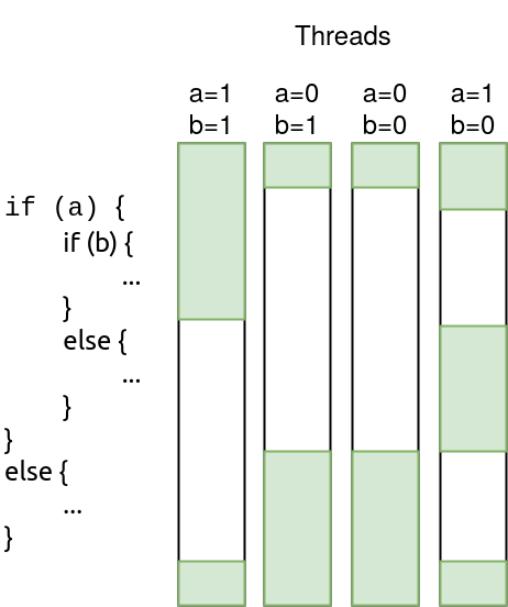
A problem that this design causes is that when executing a conditional branch, even though the program is the same, the control flow may diverge for two different threads within the same thread vector. So how does it work when the scheduler can only dispatch one instruction at a time? The solution is to simply decode every instruction (i.e., execute both branches when dealing with an if-else pattern, for instance) and add an active mask stack to each thread context to keep track of which branch is supposed to be executed.
So let’s say the GPU is dealing with an if-else pattern, and thread 1 goes into the if branch and thread 2 goes into the else branch. When executing the branch, the scheduler will start executing the if branch, and thread 1 will have its active mask set while thread 2 will have its active mask unset, thus disabling thread 2 for this branch. When the scheduler is done executing the if branch, it then starts decoding instructions from the else branch, which means thread 1 will now have its active mask unset while thread 2 will have it set. After both branches merge, both threads will have their active mask set again.
Context Switch and Latency Hiding
Because of the SIMT model and the way GPUs are built, there is currently no place for out-of-order execution. Even though some modern GPUs are capable of very limited multiple dispatch (i.e., executing more than one instruction in a single cycle, not counting pipelining), as long as they are completely independent, a single thread will execute its instructions fully sequentially.
The issue this causes is that the execution becomes highly sensitive to pipeline stalls. Imagine a memory instruction that misses the cache: while an out-of-order CPU can hide the latency by executing instructions ahead and resolving dependencies automatically, GPUs simply do not have this ability, and the full cost of bringing data from memory back to the LSU would have to be assumed.
In order to get around this limitation, GPUs will hide instruction latencies by doing a context switch to another program. While this may seem complicated at first, a single thread vector state is actually very simple and usually only contains a shared program counter, per-thread registers and active mask, and some miscellaneous information. Therefore, a context switch is very cheap and consists more or less of changing a few lookup table indices. So whenever a program hits some sort of instruction-induced latency, the GPU will switch to another thread vector and start executing instructions for this other thread vector until another latency is hit, etc. And this way the execution resources keep being fed even though one of the thread vectors is waiting for memory.
Of course, a single GPU core can only keep track of so many thread vectors at the same time. The limit on how many thread vectors a single core can handle is called the “thread occupancy” and is an important metric when analyzing GPU performance. This thread occupancy is limited not only by some hardcoded limit but also by the amount of register each program uses. Since a GPU core has a limited amount of registers, each thread vector will allocate the thread vector’s lane count times the number of registers used by the program. And once all the registers are exhausted, the GPU core can no longer keep track of more thread vectors.
Putting it All Together
Finally, before we can look at the TeraScale architecture, let’s zoom out and look at the bigger picture of how a GPU “core” executes a program.
Up until this point it may be unclear what exactly a GPU “core” is, and the reason for that is simply that there is no formal definition of what exactly a GPU core is and how processing elements are grouped. Since each vendor has its own definition and core layout, it is important to note that the following layout and explanation describe a fictional GPU, which may or may not accurately depict an actual GPU. But even though this layout may be slightly different on a consumer GPU, the concepts remain more or less the same, and I believe this to be a good enough representation.
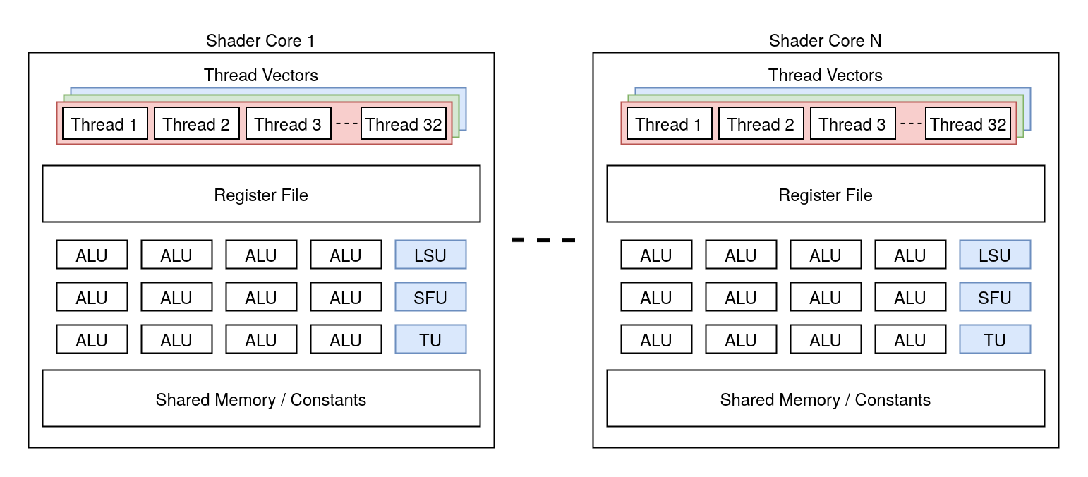
A modern GPU typically has multiple GPU cores. Each core usually contains:
- A register file: A bank of registers that will be allocated by each thread context. Some of these registers may be shared across multiple threads.
- ALUs (Arithmetic & Logic Units): The actual execution units that perform arithmetic and logic operations on the registers. Note that very confusingly, this is more or less what Nvidia calls “CUDA cores”.
- LSUs (Load-Store Units): The units responsible for memory accesses.
- SFUs (Special Function Units): These units are commonly used to perform special mathematics operations. e.g., cos, sin, exp, sqrt, etc. Note that Intel calls these EMs (for Extended Math unit).
- Texture Unit: GPU cores contain special texture units to fetch texture data. Compared to regular LSUs, these units are able to handle operations like texture wrapping, mipmapping, filtering, swizzling, etc. (Note that the texture units can sometimes be shared across multiple cores).
- Shared Memory: GPU cores usually have some sort of read-write shared memory that can be used for a variety of usages whenever data needs to be passed around.
- Constant Memory: This is also shared memory. However, some GPUs sometimes make a distinction between read-write memory and constant memory, which is read-only. This is typically where a shader’s uniform buffer ends up.
Each core manages the executions of one or more thread vectors at the same time. When busy, the GPU core instruction dispatcher starts by selecting the thread vector to execute an instruction from among the pool of thread vectors it manages. The dispatcher then fetches and issues an instruction from this program to the ALUs/LSUs/SFUs/TUs using the appropriate thread vector context (by selecting the right input/output registers, updating the program counter, potentially updating the active mask in case of a branch instruction, etc.). Once executed, the dispatcher may yield the current thread vector and pass the execution over to another thread vector if judged appropriate (e.g., if a memory request has been made and we need to wait for the result).
As previously stated, not only does every GPU vendor have its own layout, but even common terminology tends to differ (sometimes even between different architectures from a single vendor), so in order to limit confusion as much as possible, here is an attempt at making a table of GPU terminology per vendor.
Please note that this is likely not 100% accurate, as there isn’t always a 1-1 match between terms.
| Vendor | GPU Core | ALU | Thread Vector |
|---|---|---|---|
| Nvidia | Streaming Multiprocessor Sub-Partition | CUDA Core | Warp |
| AMD | SIMD / SIMD pipeline | Stream Core (Terascale-specific name?) / ALU | Wavefront / Wave |
| Apple | Shader Core | ALU | SIMDgroup |
| Intel | Execution Unit (old) / Vector Engine (new) | ALU | Sub-group |
| Qualcomm | Micro Shader Pipe Texture Pipe (uSPTP) | ALU | Wave |
| ARM | Execution Engine | ALU | Warp |
Now that we have more background on modern GPU architecture, we can finally look at the Wii U GPU.
Wii U (8th generation, 2012)
In terms of graphics, unlike what one might have expected because of the name, the Wii U’s GPU is actually further away from the Wii’s than the GameCube’s is. And as a matter of fact, the Wii U brings the whole new concept of unified shader model that every modern GPU uses.
Indeed, the Wii U comes with a Radeon R6xx-R7xx variant by AMD (formerly ATI Technologies) that uses their TeraScale microarchitecture. The TeraScale microarchitecture is the first from AMD to introduce the unified shader model. And therefore the execution model and overall design of cores is similar to what has just been described in the previous sections.
TeraScale ISA
Shaders on the Wii U use an instruction set that clearly separates control-flow instructions from clause instructions. While the former instruction type handles jumping, subroutine calls, loops, and exporting shader outputs, the clause instructions do all the ALU, vertex/texture fetches, and memory access operations.
Note that for control-flow instructions, compared to CPU ISAs, where there are usually only a couple of condition and unconditional branch instructions that can be used, GPU branch instructions are usually much more explicit about the context in which they are used. Whereas a CPU would typically use a similar “jump if non-equal” branch instruction for both an if-else statement and a loop condition, GPUs will have different instructions.
If we take a loop statement, for instance, because each thread may potentially execute the loop body a different number of times, the instruction scheduler has to do special work to handle thread masking in the current thread vector, which would not be possible with a generic conditional branch instruction. For that reason, the ISA contains different instructions for starting a loop, ending a loop, and breaking a loop.
VLIW
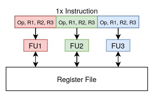
For the ALU clause instructions in the TeraScale ISA, ATI chose a VLIW (very long instruction word) format. The difference between a VLIW format and a more traditional RISC format is that a single VLIW instruction encodes multiple operations, each dispatched to its respective ALU (not to be confused with SIMD, which executes the same operation on different data). This ISA design frees the hardware from having to perform scheduling and instead relies on the compilers to exploit ILP. Note that VLIW usage is not the most widespread nowadays. Although some GPU vendors like Broadcom still use a VLIW ISA, Nvidia never used any VLIW ISA for their GPUs, and AMD moved away from VLIW when designing their next-generation GCN microarchitecture.
Geometry Shader
As we have seen in part 1, a basic graphics pipeline consists of a programmable vertex transformation stage to transform input vertex positions into screen scape coordinates, a fixed-function rasterization stage to transform polygon coordinates into pixels, and a programmable pixel processing pass to give the pixels their colors.
In addition to the vertex and fragment shaders, Terascale also supports an optional geometry shader stage. The purpose of this geometry shader is to allow programmers to generate vertices on the fly by utilizing the GPU instead of the CPU. By doing so, the programmers can save bandwidth as well as run the necessary computations in parallel.
When enabled, this type of shader intervenes between the vertex shader and the rasterization stage, and its job is to take an input vertex from the vertex shader and generate different vertices from this input to be passed to the rasterizer.
Internally, the Wii U actually uses two shaders to handle geometry shading: a geometry shader and a “DMA copy program”. Normally, when the geometry shading stage is not active, the vertex shader passes data to the fragment shader through a “parameter cache” and a “position buffer”. But when the geometry stage is active, the vertex shader writes its outputs to a vertex ring buffer instead that’s processed by the geometry shader.
Then, each vertex is processed by the geometry shader that can emit a variable amount of new output vertices per input vertex using some special instructions. The output vertices generated by the geometry shader are written to the geometry ring buffer, and that’s where the “DMA copy program” comes into play and copies all the data from the geometry ring buffer back to the parameter cache and position buffer for the fragment shader to use.
The API
In order to program the GPU, the CPU can write packets to an MMIO register. The packet format that is used is called PM4, and interestingly enough, this format is still the format used on modern AMD GPUs. PM4 packets are divided into draw packets that initiate draw operations, state management packets, and synchronization packets.
Game programmers, however, don’t have to mess with any of the details of the low-level GPU API.
Indeed, since older consoles had such unique features, the abstractions provided by the SDKs were still very close to the hardware, and programmers had to be aware of the details of the low-level API. But between the Wii and the Wii U, the hardware has gotten much more complex, and the unified shader model has provided a much more generic way of accessing the GPU. Accordingly, high-level APIs have started to become much more unified and far from the low-level APIs, making it less useful for programmers to be aware of the low-level structures.
On the Wii U, the graphics driver (called GX2) gets dynamically linked to a game by the OS, and provides a high-level interface for accessing the GPU. All the command packing and state tracking is now up to the driver and completely hidden from the game programmers, who only deal with a user-friendly interface similar to OpenGL.
The Full Pipeline
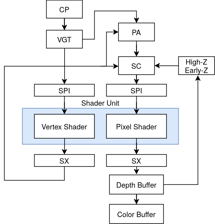
- CP (Command Processor): Processes the commands sent to the command FIFO via the write-gather pipe register.
- VGT (Vertex Grouper / Tessellator): fetches vertex and index buffers and sends them to the shader pipe interpolator (SPI) to be used by the vertex shader. The VGT also sends primitive connectivity to the primitive assembler (PA) for pixel processing.
- PA (Primitive Assembler): Receives vertex shader’s output vertex positions from the shader export unit (SX) as well as primitive connectivity from the VGT and does setup computations (i.e., edge slope and barycentric conversion coefficient computations) to be passed to the scan converter (SC).
- SC (Scan Converter): Uses the setup computations from the primitive assembler (PA) and does scanline conversion and Z testing. The resulting pixel positions and barycentric coordinates are then sent to the shader pipe interpolator (SPI) to be used in the fragment shader.
- High-Z / Early-Z: (Note that I believe “High-Z” to be a typo in the documentation given that it’s later referred to as “HiZ” for hierarchical Z.) This unit uses the depth buffer to perform Z testing. The GPU also supports hierarchical Z testing, which consists of having a down-sampled Z-buffer to make depth queries more efficient.
- SPI (Shader Pipe Interpolator): Does shader setup by allocating threads and GPRs for the shaders to be run.
- SX (Shader Export): Stores the shader computation results to be used by other units.
To recap, the Wii U follows the unified shader model and thus utilizes fully programmable shaders to perform the vertex and pixel stages of a render. In addition to the classic vertex and pixel stages, TeraScale also supports geometry shaders that use the same principle but with special instructions to generate vertices from within the GPU.
All these shader programs execute on shader cores that follow a SIMT architecture and use a VLIW ISA to be able to delegate the burden of exploiting ILP to the compiler because discovering ILP dynamically is too expensive for an architecture intended to execute massively parallel programs.
The Nintendo Switch (8th/9th generation, 2017)
The Nintendo Switch is the latest console released by Nintendo. This time, Nintendo has partnered with Nvidia, who designed the SoC used on the Nintendo Switch: the Tegra X1, which comes with a GPU (codename “GM20B”) based on Nvidia’s Maxwell microarchitecture.
Once again, the Nintendo Switch GPU follows the unified shader model, and so the same assumption about the overall architecture as described in the first section can be assumed. Even though the GPU is quite different from TeraScale, Maxwell remains in the continuity of GPU evolution. Maxwell still supports vertex, fragment, and geometry shaders but also supports new shader types. As we will see, one aspect that very much differs from TeraScale is the shader ISA itself, which is not very surprising, as shader ISA variance is very high across vendors and sometimes even across different generations from a same vendor.
On the Maxwell microarchitecture, the GPU is subdivided into so-called GPCs (Graphics Processing Clusters). These GPCs share the memory interface and an L2 cache and each contain a Raster Engine that performs primitive rasterization and multiple SMMs (Maxwell Streaming Multiprocessors).
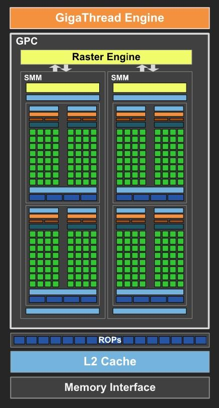
Image from Tegra X1 whitepaper.
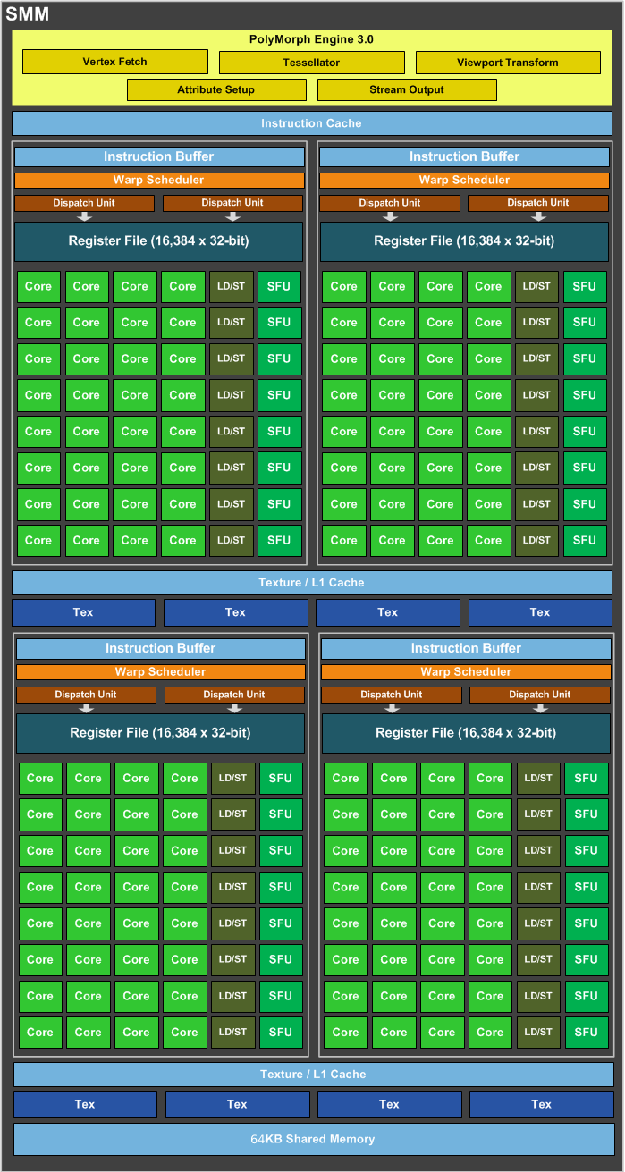
As can be observed below, one SMM consists of a PolyMorph Engine that handles the fixed-function parts of the geometry processing pipeline, as well as four SMSPs (Streaming Multiprocessor Sub-Partition), each containing a “Warp Scheduler”, and execution resources.
In Nvidia terms, a “warp” is what I referred to earlier in the SIMT section as a “thread vector”. That is, a group of threads that execute the same instruction dispatched by the warp scheduler. The actual execution resources that will perform the computations (ALUs) are what Nvidia calls CUDA cores. On Maxwell, each warp holds and manages 32 threads, which means the Tegra X1 contains 256 CUDA cores (1 GPC * 2 SMMs * 4 Warps * 32 CUDA cores).
Alongside these CUDA cores, each SM also includes LD/STs (load/store units) and SFUs (special function units), used respectively for accessing memory and computing some more complex math functions.
Tessellation
In order to cope with the high bandwidth demands of detailed geometry, DirectX 11 has added hardware tessellation as an optional stage to the graphics pipeline. What this new stage does is transform geometry with a low level of detail into higher-detail primitives. This stage allows for highly detailed geometry while keeping bandwidth and memory usage low. When enabled, tessellation is made out of three steps:
- A programmable Hull Shader (also called Tessellation Control Shader) that processes outputs from the vertex shader and generates output vertices (called patches) and tessellation factors to control how much to subdivide each patch.
- A fixed-function Tessellator that takes the outputs from the Hull shader and performs the actual subdivision.
- A programmable Domain Shader (also called Tessellation Evaluation Shader) that takes the Tessellator outputs and computes the final vertex positions.
The Maxwell ISA
Contrary to the TeraScale architecture, Maxwell doesn’t use a VLIW instruction set. Instead, a more traditional RISC-like load-store ISA is used.
An oddity (for CPU people, at least) of the Maxwell ISA is the fact that it uses a static scheduling scheme that is transparent in the binary code by explicitly encoding scheduling information generated by the compiler. For every three instructions, the assembler inserts a special instruction that contains “control codes” that describe different kinds of latencies and barriers induced by the following instructions. More specifically, these control codes include:
- A stall count that describes pipeline latency.
- A yield flag that hints the warp scheduler when the current thread can yield.
- A write dependency barrier that describes a write to the register file with a variable latency.
- A read dependency barrier that describes a read to the register file with a variable latency.
- A wait on dependency barrier to wait for a previously set barrier.
Similarly to VLIW, this design allows Nvidia to exploit ILP while saving up on transistors by not having dynamic scheduling performed in hardware. It is typically by using these hints that the warp scheduler will decide when it is best to do a context switch to avoid pipeline stalls.
The API
On a higher abstraction level, the kernel driver API is very complex compared to what we’ve seen so far. The Nvidia driver exposes a bunch of virtual files that can be opened to perform ioctls and communicate with the different interfaces (e.g., display, profiler, debug, nvmap, etc.).
Some of these interfaces share a common interface and are called “channels”. These channels are interfaces used for submitting graphics, video/jpeg encoders/decoders, etc. command lists. On the “GPU” channel for graphics, multiple subchannels are exposed to access different engines (2D, 3D, Compute, DMA, etc.). As an example, to create and submit a 3D command list, the programmer has to use nvOpen on “/dev/nvhost-gpu”, then call nvIoctl with NVGPU_IOCTL_CHANNEL_ALLOC_GPFIFO_EX, create commands with the subchannel field set to MAXWELL_B (the id of the 3D subchannel), and finally, submit the commands using nvIoctl with NVGPU_IOCTL_CHANNEL_SUBMIT_GPFIFO.
This is obviously a simplification, as there are a whole lot more ioctls to perform for initialization, memory management, etc., but the overall concept remains the same.
On the userland side, Nintendo and Nvidia developed their own proprietary graphics API called NVN, which is quite close to Vulkan. The userland driver (which is embedded in the SDK) communicates with the kernel driver through the exposed virtual files and sends the command lists that it crafted while receiving the NVN calls from the game.
The Full Pipeline
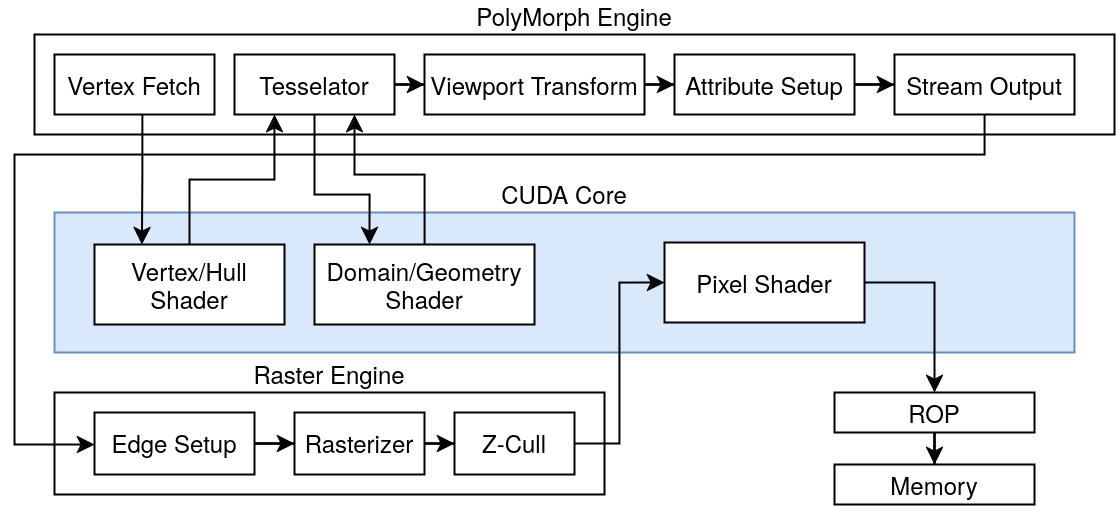
- Vertex Fetch: First, the PolyMorph engine fetches the vertices from memory and sends them to the Vertex Shader for vertex transformation.
- Hull Shader: When tessellation is enabled, the resulting vertices are sent to the Hull Shader.
- Tessellator: The Hull Shader’s outputs are then sent to the Tessellator to subdivide the geometry.
- Domain Shader: The Tessellator then sends the output control points to the Domain Shader to emit the final tessellated vertices.
- Geometry Shader: When the Geometry Shader stage is enabled, the vertices are sent to the Geometry Shader that emits the final vertices.
- Viewport Transform: The resulting vertices are sent to the viewport transform unit, which performs clipping, viewport transformations, and perspective correction.
- Attribute Setup: This unit will process the interpolants and generate plane equations to be used by the rasterizer.
- Edge Setup: Resulting vertices and attributes are then sent to the raster engine that computes edge equations for scanline conversion. This stage also performs back face culling.
- Rasterizer: This unit does the scanline conversion to determine which pixel gets drawn.
- Z-Cull: Covered pixels then get tested against the Z-buffer.
- Pixel Shader: The resulting pixels and interpolated attributes are then sent to the pixel shader to compute the final color value.
- ROP: Once the pixels are processed, they are sent to the ROP (Render Output) unit, which performs anti-aliasing and writes color/depth values back to the color/depth buffer by communication with the memory interface.
Nintendo Switch 2 (9th generation, 2025?)
At the time of writing this article, the successor to the Nintendo Switch has not been released or even announced yet. However, it appears more than likely that this console will come with a GPU based on Nvidia’s Ampere microarchitecture (not to be confused with Ampere Computing).
On an architectural level, Ampere still being an Nvidia GPU, the overall layout isn’t fundamentally new, and a lot of units are still either very similar or an evolution over Maxwell. There are, however, a few novel additions that mostly inherit from the Turing microarchitecture: Ampere’s predecessor.
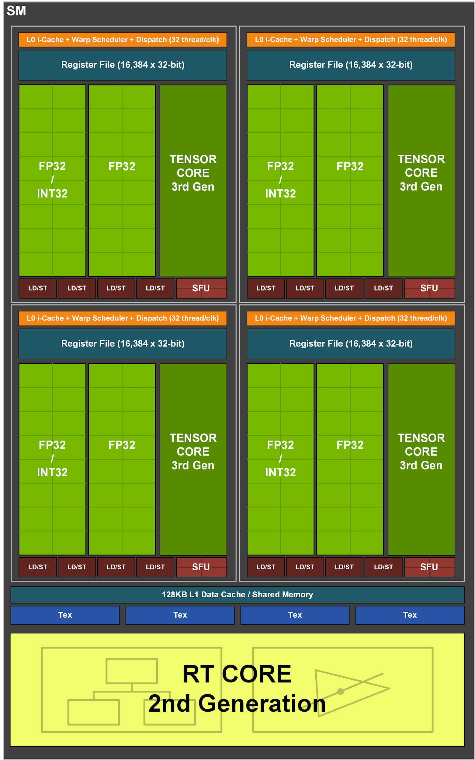
Image from Ampere whitepaper.
Compared to Maxwell, a first noticeable difference is that the “CUDA cores” are now separated between FP32/INT32-capable and only FP32-capable cores. Doing so allows the GPU to execute both FP32 and INT32 operations at the same time, whereas on Maxwell, only one datapath had to be chosen while the other would be left idling.
The most important difference, however, is the addition of two new hardware units: the Tensor and RT cores, which are respectively used for AI and ray tracing.
Ray Tracing
With the rasterization model, lighting calculations follow some approximation models that yield pretty good results, but that are still approximations that sometimes fail to account for some interactions that, if added, would add more realism to our scenes.
Ray tracing is another rendering technique that tries to make lighting calculations closer to what actually happens in the real world. With ray tracing, instead of shading pixels on a per-geometry basis like on the rasterization model, we instead shoot rays from a camera view plane into a scene and then shade the pixels based on the closest geometry that intersects with the generated ray. This notably allows programmers to easily compute reflection and refraction on materials by shooting rays recursively from a ray and geometry intersection point, whereas with the raster model we would have to rely on other tricks like dynamic environment mapping.
The main issue with ray tracing on previous GPUs is that it’s rather expensive to implement without proper hardware support, rendering its use unsuited for real-time rendering. Which is why there has been interest in adding hardware acceleration for this technique: Starting with AMD’s RDNA2 microarchitecture and Nvidia’s Turing microarchitecture, GPUs have started including ray tracing cores to be used in a new pipeline.
The way this new ray tracing pipeline works is by introducing four new shader types:
- A ray-generation shader responsible for casting rays.
- An intersection shader (optional) that computes intersection with user-defined geometry.
- An any hit shader (optional) that processes further the intersection and can perform, for instance, alpha testing with the intersected geometry.
- A closest hit or miss shader that determines the action to take upon the ending of an intersection search.
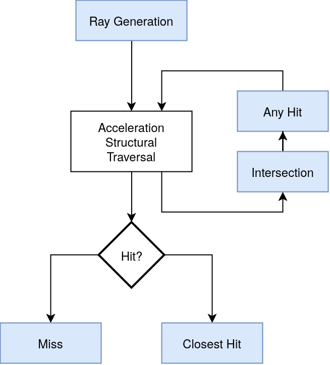
These new shaders are executed on the regular GPU cores while the new RT cores handle the fixed-function parts. Nvidia RT cores on Ampere are divided into two units. The first unit is responsible for testing bounding boxes, while the second does intersection testing between generated rays and triangles.
Acceleration Structure
During a ray tracing pipeline, since the hardware has to perform lots of intersection tests between generated rays and primitives, the CPU has to upload the scene geometry to the GPU, which can later be traversed by the RT cores.
But instead of directly using a plain array of scene primitives and iterating over all of them until an intersection is found, the GPU will usually need a pass to construct a more efficient data structure referred to as a “ray tracing acceleration structure”.
Multiple types of data structures exist for this purpose, but the most popular choices are based on bounding volume hierarchies (abbreviated BVH). Game engine developers, however, do not have to worry about the low-level structure as they can simply provide an API-abstracted version of the scene to the graphics driver, which then takes care of building the acceleration structure.
Sadly, when it comes to the low-level details, Nvidia does not disclose much, as this is still very new. The actual BVH structure, as well as how it is constructed, are not documented, but it is likely that this part is done on the CUDA cores by a built-in shader invoked by the graphics driver.
As for the RT cores access, the ISA likely provides some special instructions to dispatch intersection test work to the RT cores. Because of the tree structure of BVHs, the traversal process implemented in the RT cores essentially consists of managing a stack that gets updated to keep track of which node is currently being processed until a leaf node gets reached. But again, the exact stack’s inner workings are not known.
Ray Tracing Divergence Problem
Although ray tracing allows developers to perform more advanced lighting calculations at a reduced cost, there is also an interesting side effect of the ray tracing model that has potential performance implications. Indeed, some aspects of ray tracing are incompatible with the way modern GPUs were built and optimized, and that is because the ray tracing pipeline is highly prone to data and code divergence.
As seen in the SIMT section, GPUs are great at executing lots of threads that do the same computations at the same time. But let’s say a lot of threads that perform different computations are invoked together. The shader cores will have a very low lane occupancy (i.e., the number of lanes active in a single thread vector), which means lots of the execution resources will actually stay idle when dispatching a thread vector instruction, which is very inefficient.
This low lane occupancy stems from the fact that when generating rays from the view plane, even pixels that are close to each other may end up having their rays bounce on totally different objects with different shaders to execute. On the raster model, however, since the work is separated on a per-geometry basis, grouping threads together is trivial: all the pixels in a primitive will execute the same shader.
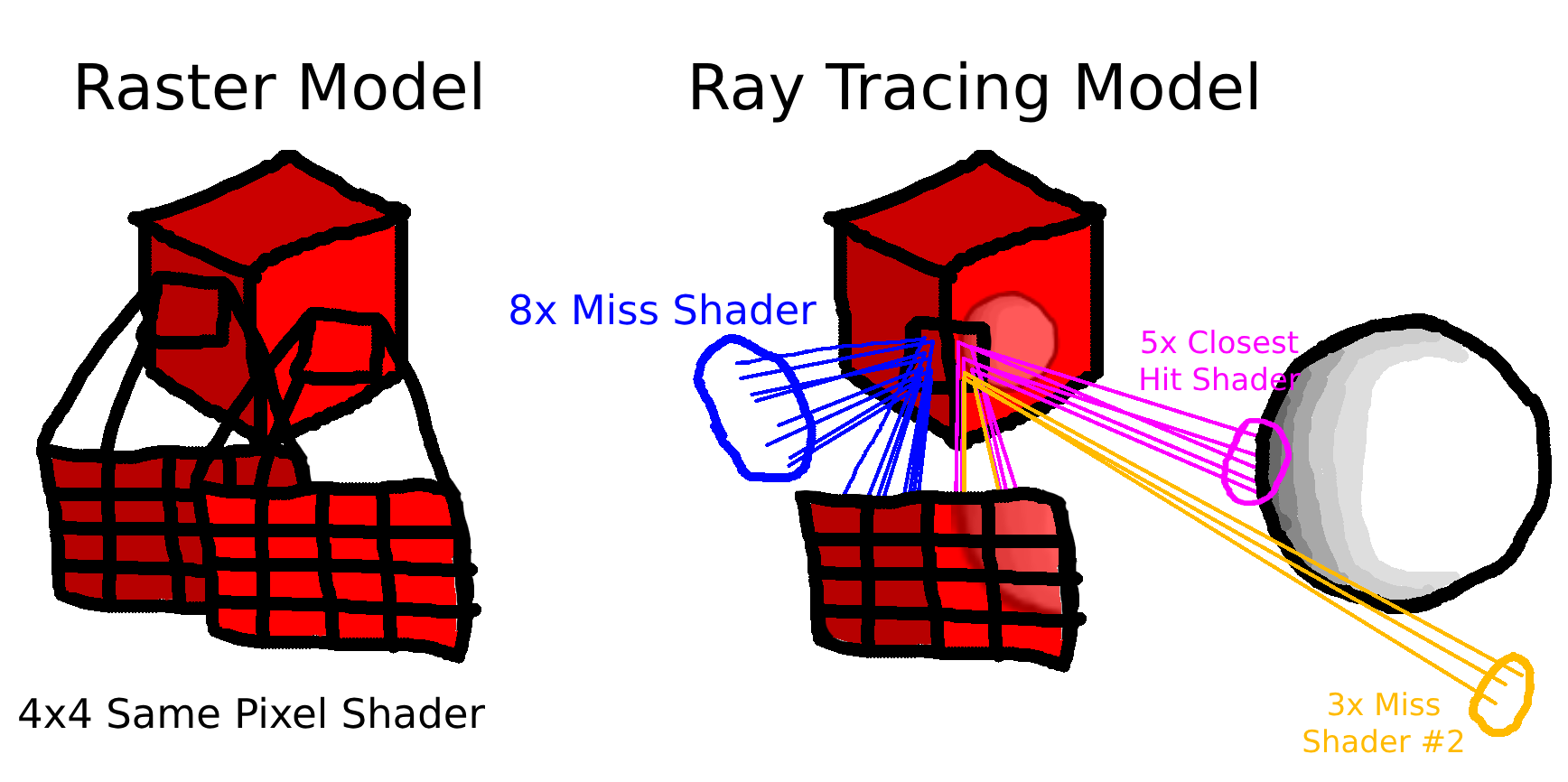
If we take the above example, with the raster model, the 4x4 pixel square that we’re trying to render will be easily handled in a single shader invocation since we’re processing a single primitive that uses the same shader for all of its fragments. On the ray tracing model, however, we start by launching rays from the view plane, and we first hit the cube, which invokes a closest hit shader, which is the same for all the fragments. However, when computing the reflection, the rays diverge drastically in different directions, and we can end up having to schedule three different shader invocations, each having a low lane occupancy (8, 5, and 3 in the example).
Lane occupancy is not the only divergence-related problem. It’s also possible for a single shader to perform poorly if the data it accesses is incoherent, as this may induce higher branch divergence and reduce the cache’s ability to exploit spatial locality.
Tensor Cores and DLSS
The other big addition to the Turing architecture, which is also present in Ampere, is the Tensor cores. These Tensor cores are used to implement fast INT4/INT8/FP16 matrix multiplication and are accessible through special shader instructions. In practice, these cores are really just used for AI workloads, since AI heavily relies on matrix multiplications.
In the context of computer graphics, these Tensor cores are used for Nvidia’s Deep Learning Super Sampling algorithm: DLSS. The idea behind DLSS is that rendering is getting increasingly more expensive as we move towards real-time photorealistic rendering, and so DLSS tries to accelerate the process by rendering a downsampled image and then upscaling it using AI.
If we look at how this is all implemented in DLSS 2.0 (the version supported by Ampere; other versions work a bit differently), Nvidia has an AI model that was pretrained and that takes as input:
- A downsampled image: a regular framebuffer rendered at a fraction of the final resolution before any post-processing effects have been applied to it.
- A motion vector: a texture generated by computing pixel displacement between the last frame and the current frame. This can be easily generated by keeping track of the last WVP matrix of each object in the scene and checking the difference for each pixel.
- A viewport jitter: a small offset that was applied to the viewport.
- A depth buffer: a regular depth buffer generated from the render.
From a programmer’s perspective, once the above input parameters have been generated, the code can call an API function with these parameters that will return the upscaled frame. How exactly the low-level invocations occur is quite opaque and not really documented, but what’s likely happening is that the driver contains a proprietary compute shader that utilizes the tensor core instructions to run the AI model inference, and that is invoked by the graphics driver.
Mesh Shading
On the raster model, the geometry pipeline has also benefitted from new features. The Turing architecture has added a brand new pipeline meant to replace the traditional Primitive Assembly -> Vertex Shading -> Tessellation -> Geometry Shading pipeline.
As the amount of scene geometry is starting to grow, the fixed-function stages in the pipeline have started to show their limitations. Prior to mesh shading, through their APIs, the command processors would typically expose a way to provide vertex/index buffers and some structures to describe the vertices attributes. The programmers would then be able to perform vertex transformation on a per-vertex basis and eventually generate some more vertices with a tessellation/geometry shading stage. But anything that happens in between (fetching the vertices, assembling primitives, actually dividing the geometry for tessellation, etc.) would remain hidden and handled internally by the GPU through fixed-function hardware.
Mesh shading changes this design and lets the programmers have total control over the entire geometry processing stage. Instead of having different shader types interleaved with fixed-function stages, the mesh shading pipeline provides a replacement that only consists of two shader types:
- A Task shader that divides the work and controls sub-invocations (comparable to a hull shader in the tessellation stage)
- A Mesh shader that actually performs all the work to fetch the vertices and output the final primitives.
With this level of control, it becomes much easier to not only reduce the vertex bandwidth by implementing custom geometry compression, packing, or generation, but also to better divide the work across the cores.
Conclusion
As seen in this article, GPUs are fascinating and very complex systems. And therefore, there have been a lot of evolutions throughout the years to go from layer-based 2D compositors to the insanely complex multipurpose systems they are today.
And even though this article tried to cover enough to have a decent understanding of the internals without getting too boring, there is still a lot more to talk about, especially given the high implementation variance across GPU vendors.
Additionally, as stated in the introduction, only the graphics part was covered in this, and modern GPUs have more units dedicated to other tasks.
To give some pointers, here is a nonexhaustive list of related subjects an interested reader can look at:
- Upscaling artifacts (e.g., ghosting)
- Ray tracing noise problems
- GPU memory hierarchy
- Tile-based renderers in mobile GPUs
- DDR vs. GDDR
- Display/video engines
One very unfortunate aspect for us, however, is that most of the time it’s quite difficult to figure out exactly how modern GPUs work internally because of the little amount of low-level documentation available and the lack of open-source implementations.
Some GPU vendors, like AMD and Intel, do try to document some parts of their internals by publishing ISA specifications, providing open-source drivers, etc. But most vendors barely provide any documentation that goes deeper than marketing terms, and end up only documenting the API.
This makes understanding their architecture in-depth very difficult, as it requires relying on either reverse engineering projects or reading between the lines and speculating off of the limited available material. Something I personally hope will change, both for the quality of the overall ecosystem and my own curiosity.
Glossary
ILP
ILP (instruction-level parallelism) refers to the ability of a sequence of instructions to be executed in parallel. Two instructions can be run in parallel if they don’t depend on each other. For a processor to achieve maximum performance, it has to exploit ILP in an instruction stream to be able to execute as much code as possible in a given time span. Note that ILP may highly depend on the ISA design.
More here.
DMA
Direct Memory Access refers to when a hardware unit does some sort of memory transfer. This can essentially be seen as a hardware memcpy.
Mipmapping
Sampling high-resolution textures for objects that appear small on screen wastes bandwidth and produces artifacts. Mipmapping consists of storing not only the original version of a texture but also downsized versions of that same texture in memory. And when the GPU needs to access the texture, it will choose the version that’s used depending on how far from the camera the object is.
More here.
Texture Swizzling
Because textures are two-dimensional arrays, spatial locality is quite different from a one-dimensional representation. Indeed, if we take a pixel at coordinate P1=(x, y), the pixel at P2=(x+1, y) is a neighbor pixel, but so is the one at P3=(x, y+1). If we were to store a texture in memory the same way we would with a two-dimensional C array (i.e., coordinate (x, y) maps to index y * width + x), we would have terrible performance when traversing a texture on the y-axis because P1 and P3 are much less likely to be in the same cache line than P1 and P2.
Texture swizzling, also called tiling (but not to be confused with vector swizzling), is a technique that was developed in order to get around this issue. The idea is that instead of storing a texture row by row in memory, the texture is divided into N * N tiles, and the pixels within these tiles are adjacent in memory. This way every pixel within a single tile fits in a single cache line, and thus a new cache line needs to be accessed when crossing a tile boundary instead of potentially at every single row.
Hierarchical Z-Buffer
Hierarchical Z-Buffering is a technique that consists of having downsampled versions of the full Z-buffer. Having these downsampled versions allows the hardware to do more efficient depth queries. This comes from the fact that a smaller buffer size improves spatial locality and thus increases the cache hit rate.
More here.
Dynamic Environment mapping
Dynamic environment mapping is a technique that consists of rendering an object’s surroundings dynamically, typically to apply reflection and refraction effects. The main issue with this technique is that rendering the scene from multiple angles for each object is simply not feasible. The performance impact usually causes game engine developers to use a mix of static (pre-computed) and dynamic environment mapping, which may result in some dynamic objects not being taken into account in some objects’ reflection/refraction.
More here.
Bounding Volume Hierarchy
A bounding volume hierarchy is a tree data structure where each object in the scene is a leaf node, and all the other nodes represent a bounding volume in the scene containing all its subnodes. Keeping the objects in such a data structure makes some algorithms (such as collision detection or ray tracing) much more efficient than iterating over all the objects all the time.
More here.