Introduction
In the world of modern computing, semiconductor chips are marvels of engineering that push the boundaries of human ingenuity. As we race towards smaller, faster, and more efficient processors, with transistors now measured in mere nanometers, we encounter a fascinating paradox: perfection at this scale is nearly impossible to achieve. The result? Your CPU, the brain of your computer, is likely “broken” — at least partially.
This article explores the intricate world of chip binning, a crucial process in the semiconductor industry that turns imperfection into innovation. We will dive into the complex manufacturing process, the mechanics of chip binning, advanced testing techniques, and the economic implications of this practice.
1. The semiconductor manufacturing process
A close look at a CPU shows a stack of electronic circuits and insulating materials. At the bottom are transistors, which act as logic gates. Above them is the first layer of metal wires that connect the transistors in a specific circuit pattern. Layer by layer, more circuits are added. In modern processors, there are usually about 12 to 15+ layers of circuits stacked above the transistors, separated by insulating materials.
![]()
Rendering of a small standard cell with three metal layers. Insulation has been removed. Circuit patterns are stacked one on top of the other. (from wikimedia.org)
Manufacturing a semiconductor requires hundreds of steps over several months. At the very beginning, silicon, the primary material for most chips, is refined from sand and formed into wafers.
 Wafers before engraving. (from okmetics.com)
These wafers then go under several industrial processes, including:
- Photolithography: Patterns of circuits are etched onto the wafer using light-sensitive chemicals and masks.
- Deposition: Layers of materials like metals or insulators are deposited on the wafer.
- Etching: Unwanted material is removed, leaving behind intricate circuit patterns.
These essential steps are repeated again and again to create dozens of layers of material.
Each of these steps must be aligned perfectly. Any minor misalignment, impurity, or defect can affect the final chip’s performance.
 An etched wafer of 4th generation Intel series, but not yet split into individual chips. (from wikimedia.org)
If interested, the first 10 minutes of this video covers this topic in detail: https://youtu.be/dX9CGRZwD-w
2. The role of chip binning
2.1 What is chip binning?
Chip binning is the process of sorting and classifying chips after manufacturing based on their performance and characteristics. Not all chips that roll off the production line can meet the highest performance specifications, but rather than discarding imperfect chips, manufacturers sort them into “bins” based on their capabilities. These bins typically correspond to different clock speeds, power consumption, or thermal characteristics.
For example, a wafer designed to produce an 8-core CPU might have some chips where one or two cores do not meet the required specifications. Instead of throwing these chips away, manufacturers will disable the faulty cores and sell the chip as a 6-core CPU.
TechSpot, in a January 2024 article by Nick Evanson, shows that in attempting to manufacture its i9-10900 processor, Intel will produce chips that will ultimately correspond to one of 19 different models due to binning.
| Model | # Cores | # Threads | Base clock (GHz) | All core turbo (GHz) | Turbo boost (GHz) | PL1 TDP |
|---|---|---|---|---|---|---|
| i9-10900K | 10 | 20 | 3.7 | 4.8 | 5.1 | 125 |
| i9-10900KF | 10 | 20 | 3.7 | 4.8 | 5.1 | 125 |
| i9-10900 | 10 | 20 | 2.8 | 4.5 | 5.0 | 65 |
| i9-10900F | 10 | 20 | 2.8 | 4.5 | 5.0 | 65 |
| i9-10900T | 10 | 20 | 1.9 | 3.7 | 4.5 | 35 |
| i7-10700K | 8 | 16 | 3.8 | 4.7 | 5.0 | 125 |
| i7-10700KF | 8 | 16 | 3.8 | 4.7 | 5.0 | 125 |
| i7-10700 | 8 | 16 | 2.9 | 4.6 | 7.7 | 65 |
| i7-10700F | 8 | 16 | 2.9 | 4.6 | 4.7 | 65 |
| i7-10700T | 8 | 16 | 2.0 | 3.7 | 4.4 | 35 |
| i5-10600K | 6 | 12 | 4.1 | 4.5 | 4.8 | 125 |
| i5-10600K | 6 | 12 | 4.1 | 4.5 | 4.8 | 125 |
| i5-10600 | 6 | 12 | 3.3 | 4.4 | 4.8 | 65 |
| i5-10600T | 6 | 12 | 2.4 | 3.7 | 4.0 | 35 |
| i5-10500 | 6 | 12 | 3.1 | 4.2 | 4.5 | 65 |
| i5-10500T | 6 | 12 | 2.3 | 3.5 | 3.8 | 35 |
| i5-10400 | 6 | 12 | 2.9 | 4.0 | 4.3 | 65 |
| i5-10400F | 6 | 12 | 2.9 | 4.0 | 4.3 | 65 |
| i5-10400T | 6 | 12 | 2.0 | 3.2 | 3.6 | 35 |
The CPU’s “Base clock” (GHz) represents its minimum operating frequency under any load. “All core turbo” is the highest frequency all cores can simultaneously achieve, though not necessarily sustain. “Turbo boost” is similar but applies to only two cores.
PL1 TDP (Power Level 1 - Thermal Design Power) indicates the heat generated by the CPU at its base clock under any load.
Suffixes in CPU model names indicate specific features: “F” signifies a disabled GPU, “K” an unlocked clock for overclocking, and “T” designates a low-power variant.
Overall, as we move further down the table, the CPU specifications tend to worsen.
2.2 Why do manufacturers do chip binning?
Binning allows manufacturers to maximize the number of chips produced from each wafer, ensuring that even lower-performing chips are sold rather than thrown away. It is especially critical in the semiconductor industry because manufacturing costs are extremely high, and a lot of the expense goes into the silicon wafer itself. By binning chips, manufacturers can produce multiple product tiers from a single design, optimizing the economics of chip production.
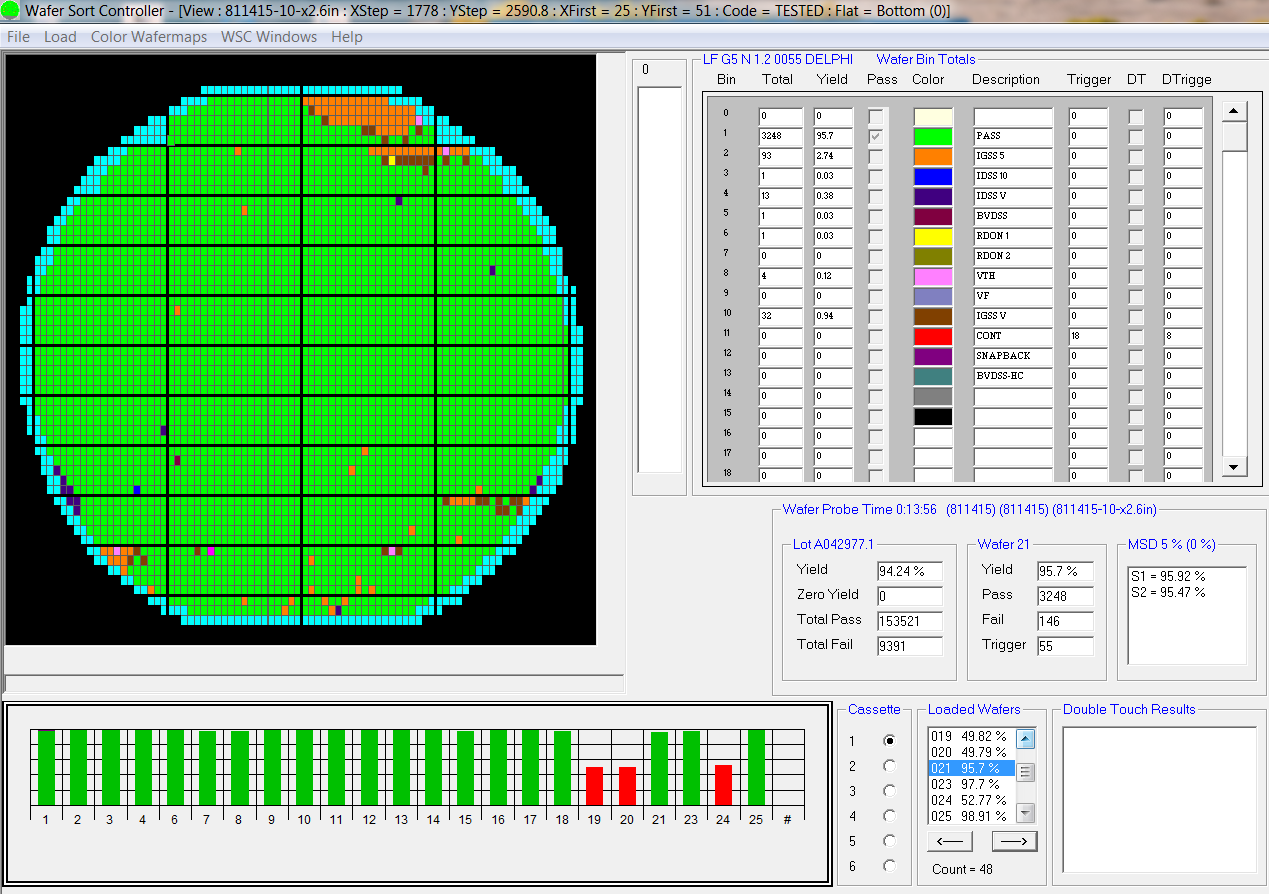
 Screenshot of wafer binning map software showing test results with different colors for different chip grades. (from blackboxsoftwaresolutions.com)
3. How chips are tested?
In order to do precise and accurate binning, chips must undergo rigorous testing. Many techniques are used to test these chips, and it starts even before manufacturing, right from the design phase. This section delves into the technical details of various testing techniques. Feel free to skip ahead if this is not your cup of tea.
3.1 Design for Testability
Design for Testability (DFT) is an important step in the process of designing a semiconductor. DFT works by embedding test features into the chip during the design phase. These features act as “windows” into the chip, allowing engineers to see what is happening inside. They include added circuits or connections that give access to signals or parts of the chip that are otherwise inaccessible.
It aims at ensuring that chips can be tested for defects after manufacturing. With these features in place, engineers can probe and manipulate specific parts of the chip to ensure they are working as expected. These tests help catch potential issues early, ensuring that the final product performs as intended.
3.2 Scan testing
One of the most common testing techniques enabled by DFT is scan testing. In this method, the memory elements within a chip — such as flip-flops or registers — are organized into scan chains, allowing engineers to shift test patterns into the chip. These scan chains function like a conveyor belt: each bit in the test pattern (a sequence of 0s and 1s) is placed onto the belt, and with each clock pulse, the bits are shifted along the chain until the entire test pattern is loaded into the chip.
Once the test pattern is fully loaded, the chip is run for a brief moment under normal operating conditions (this is called the capture cycle). During this time, the chip behaves as it normally would, processing the input signals. Afterward, the results of this operation are captured and shifted back out of the chip through the scan chains, where they are compared to the expected output. If the results match, the chip has passed the test; if not, a defect is present.
 Scan testing.
This technique is effective because it allows engineers to control and observe what is happening inside the chip, even at its most deeply embedded points, without needing to probe each individual logic gate directly.
3.3 Stuck-at faults: a use case of scan testing
A stuck-at fault is a typical issue in digital circuits that can be tested with scan testing. It occurs when a signal or pin in a circuit is stuck at a constant value — either a logical 0 or 1 — due to manufacturing defects, preventing it from switching as it should.
A stuck-at fault occurs in digital circuits, particularly in combinational circuits made up of logic gates like AND, OR, and XOR. These gates do not have memory, meaning their outputs depend only on the current inputs, not on any past values.
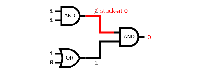
To detect such faults, we use test patterns as explained before. For example, if you send two 1s to test an AND gate and it outputs something unexpected (a 0), you know there is a problem.
 Example of a stuck-at fault. The first AND gate is stuck at 0 which corrupts the final output.
This testing model was very effective for older technologies like TTL. TTL stands for Transistor-Transistor Logic, a technology used in the 1970s and 1980s for building circuits. TTL circuits use transistors to create logic gates that switch between 0 and 1. These circuits were popular because they were fast and reliable.
In modern circuits, we now use CMOS technology. CMOS stands for Complementary Metal-Oxide-Semiconductor, which is a more advanced type of transistor used in most chips today. CMOS circuits are more power-efficient than TTL, but they also experience different types of faults. For example, stuck-open faults (where a transistor does not switch) or bridging faults (where signals between adjacent wires interfere with each other) can occur. These faults require more complex testing methods beyond the simple stuck-at testing model.
3.4 Iddq testing
Because of the transition from TTL to CMOS technologies in modern circuits, testing methods had to evolve to be able to test new fault types. One such testing method is Iddq testing, which stands for “quiescent current testing.” This method targets CMOS integrated circuits and focuses on detecting manufacturing faults by measuring the supply current, known as Idd, in a state where the circuit is quiescent — meaning it is not actively switching, and the inputs are held static.
The core principle of Iddq testing lies in the expectation that a correctly functioning CMOS circuit consumes almost no current in its quiescent state, except for a minor amount of leakage current. CMOS circuits are designed so that, during quiescence, there is no continuous path between the power supply (Vdd) and ground (GND). However, many manufacturing faults — such as gate oxide defects, short circuits, or bridging faults — can create unintended current paths, significantly increasing the Iddq value. This current spike is what Iddq testing identifies, making it a powerful tool for catching defects with a single measurement. Additionally, Iddq can detect faults that might go unnoticed using the traditional stuck-at test technique, such as shorts between adjacent transistors or power rails.
4. Cost and efficiency in binning
Chip binning, while beneficial, introduces several costs that motivate research into cost-reduction techniques.
4.1 Why binning is expensive?
One of the primary factors driving up the cost of chip binning is the timing of critical tests, particularly speed testing (testing the maximum operating frequency). Many of these tests are performed after the chip has been packaged, rather than at the wafer level. This late-stage testing is necessary because wafer-level testing has limitations in accurately measuring high-speed performance, and packaged chips provide a more realistic environment for speed testing. The consequence of this approach is that resources are often wasted on packaging chips that may not ultimately meet performance requirements.
The increasing adoption of advanced packaging techniques, such as 2.5D and 3D packaging, further increases the cost issue. These complex packaging methods are expensive in themselves, and discovering that a chip does not meet specifications after it has been packaged results in a greater financial loss.
Finally, the precision requirements of modern chip applications add another layer of expense to the binning process. Some applications require very precise binning, which necessitates the use of more sophisticated testers, which are more expensive to purchase and maintain. These precision tests also often take longer to perform, reducing throughput and increasing cost per unit.
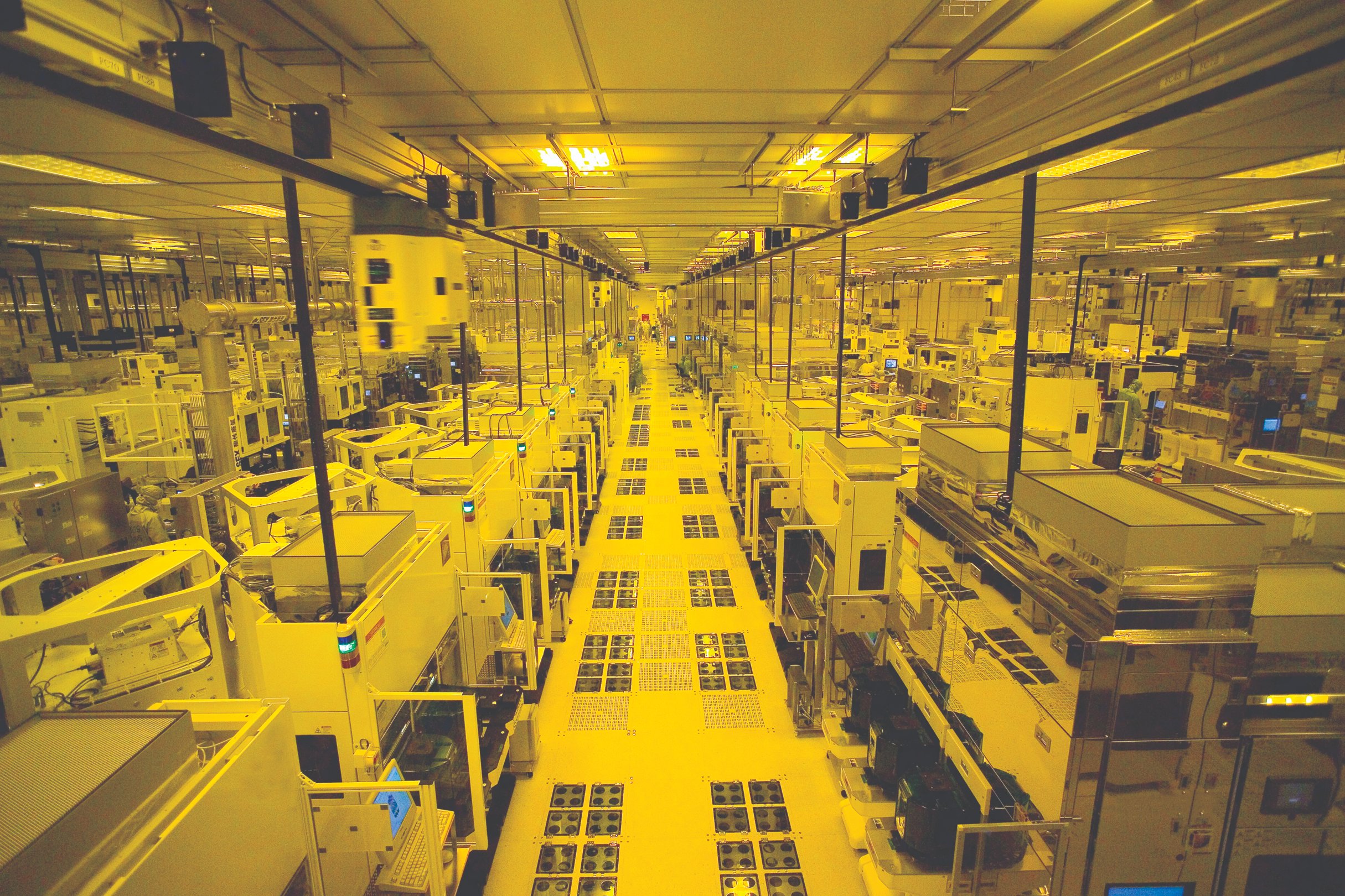
 Inside TSMC’s fab: The rising complexity of semiconductor designs requires more advanced and costly machines for manufacturing and testing. (from tsmc.com)
4.2 Reducing costs with testing optimization
Modern chips contain millions or even billions of transistors, which makes exhaustive testing with long, detailed test patterns impractical. Test compression solves this problem by reducing the amount of data that needs to be shifted in and out during testing, saving both time and money.
Compression works by using a smaller, compressed test pattern, which is then expanded on the chip itself to cover all the necessary internal pathways. This is often achieved with specialized decompression logic built into the chip. The compressed test pattern is fed into this decompression logic, which expands it into a larger set of test vectors. On the output side, response compression is used to condense the test results into a smaller data set before shifting them out of the chip. This way, the test time and memory requirements are significantly reduced while still maintaining a high level of fault coverage.
4.3 Repairing chips to save money
When a chip is detected as faulty, manufacturers collect detailed failure data such as which part of the chip failed and how. It becomes easier to identify the source of the problem and in some cases, even repair the chip.
For most consumer-grade chips, repairing a defective chip is not feasible. If a chip fails its post-manufacturing tests, it is usually discarded or binned into a lower-performance product category. However, in certain cases, limited repairs are possible, especially for specialized or high-cost devices.
For instance, in the case of embedded memories, some chips are designed with extra, redundant memory rows or columns. If a defect is found in one of the memory cells, the faulty section can be “repaired” by rerouting operations to the redundant elements. This process, called memory repair, can be done automatically through Built-In Self Repair (BISR) mechanisms or manually at the factory.
In more advanced systems, such as multi-chip modules (MCMs), systems-on-chip (SoCs) or printed circuit boards (PCBs), repair can involve physically replacing or reconfiguring faulty components. In this context, DFT plays a role in identifying exactly which chip or component is faulty, allowing technicians to replace only the defective part instead of scrapping the entire module.
4.4 New cost reduction techniques
New techniques are being developed to further reduce the cost of binning. One promising approach is the concept of “early and fine binning”, which uses new data sources to gain visibility into chip performance at much earlier stages of production. Companies have developed systems that enable manufacturers to perform “virtual binning” based on deep data analytics. This approach uses a combination of tiny on-chip test circuits and AI software to find relationships between a chip’s internal behavior and the parameters measured during standard testing processes.
The key advantage of this early binning approach is that it allows manufacturers to predict chip performance characteristics at the wafer sort stage, long before packaging. By avoiding the packaging of chips that will not meet performance requirements, manufacturers can substantially reduce waste and reduce their costs.
Conclusion
Your CPU is likely “partially broken” due to the incredible complexity of manufacturing billions of transistors on a tiny silicon chip. However, through chip binning, these imperfections become an advantage. Manufacturers rescue partially defective chips by disabling faulty components or reducing clock speeds, maximizing yield, and offering diverse products at various price points. This pragmatic approach turns the challenges of semiconductor fabrication into an opportunity, ensuring that even “imperfect” chips can efficiently power our digital world. The next time you use your computer, remember that its brain, while not perfect, shows how human ingenuity has overcome the limitations of cutting-edge technology.
Bibliography
https://www.techspot.com/article/2039-chip-binning/
https://www.youtube.com/watch?v=dX9CGRZwD-w
https://en.wikipedia.org/wiki/Integrated_circuit
https://en.wikipedia.org/wiki/5_nm_process
https://en.wikipedia.org/wiki/Stuck-at_fault
https://en.wikipedia.org/wiki/Design_for_testing
https://en.wikipedia.org/wiki/Iddq_testing
https://semiengineering.com/early-and-fine-virtual-binning/
https://www.semianalysis.com/p/clash-of-the-foundries
https://www.techspot.com/article/1840-how-cpus-are-designed-and-built-part-3/
https://static.aminer.org/pdf/PDF/000/282/891/dynamic_data_bit_memory_built_in_self_repair.pdf