The miniaturisation of electronics applied to sensors
Scope of this article
This article is a review about the miniaturisation of electronics applied to the field of sensors, and its possible future uses and evolutions. I chose to focus on one type of microsensor to present a more concrete idea of what microsensors can look like. I do not plan to dive into the details of the operation of microchips as it would make this article too heavy to read and to understand for an unsuspecting public. Nevertheless, we will see how component layers in a microsensor can be organised.
Introduction
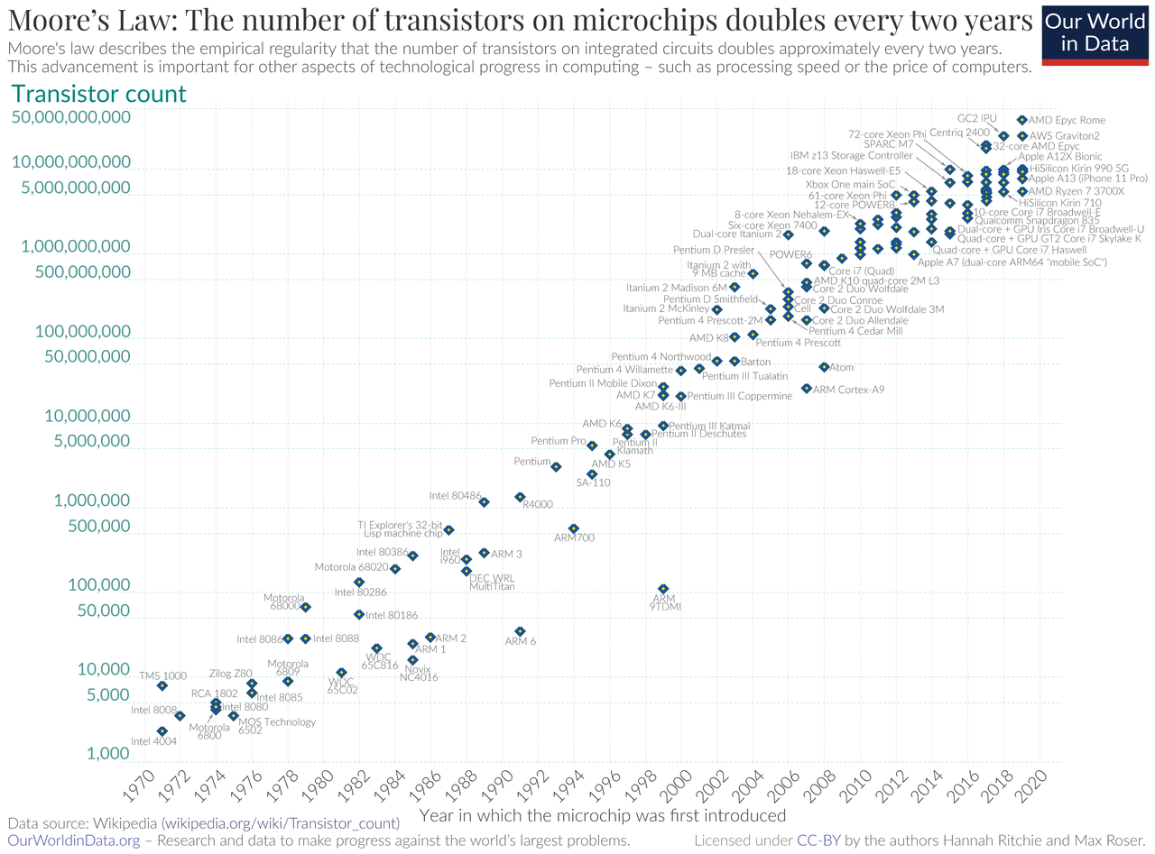
You might have heard about Moore’s law, which states that the number of transistors, the most basic components of computer logic circuits, doubles every two years. A consequence of this law, called Bell’s law, states that roughly every decade a new class of computers appears, along with new usages and possibilities. The main responsible for these recurrent breakthroughs is mainly the work done in the miniaturisation field.
Since the beginning of the history of electronics, scientists have been busy searching for solutions for shrinking the size of components, often too space-consuming for their dream contraptions. They have made a lot of progress in the miniaturisation field, enough to reach a point where fully functional computers can be hardly visible.
Why is there a need for miniaturisation?
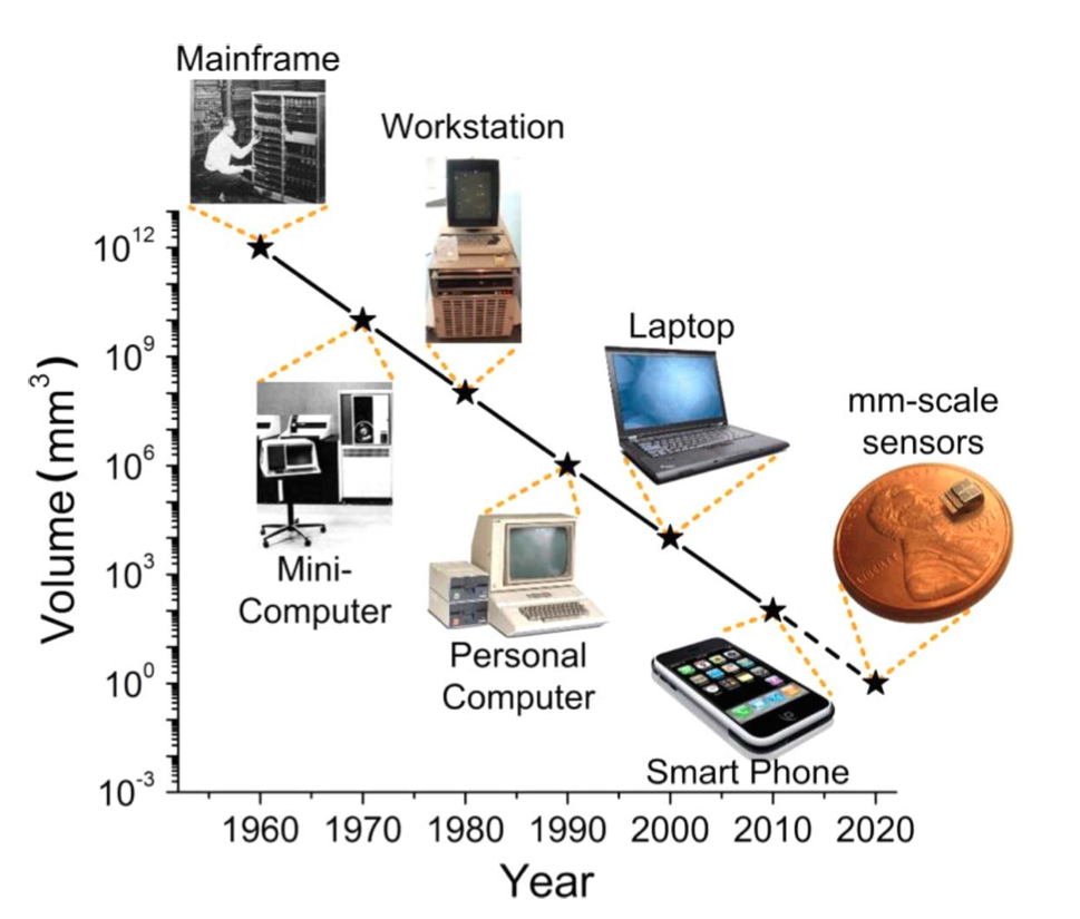
Since the birth of electronics and information technologies, miniaturisation stands out as a driving force behind innovation and progress. It has always been a field in which technologies could be improved, but our 21st century society emphasises this relentless pursuit of smaller components. Indeed, in the middle of the 20th century, computers were certainly imposing, and not everyone could buy one because of it. The need to shrink their size seemed more obvious at that time than today. However, with the rise of personal electronic devices such as cellular phones, and later smartphones, miniaturisation is still a major field of research.
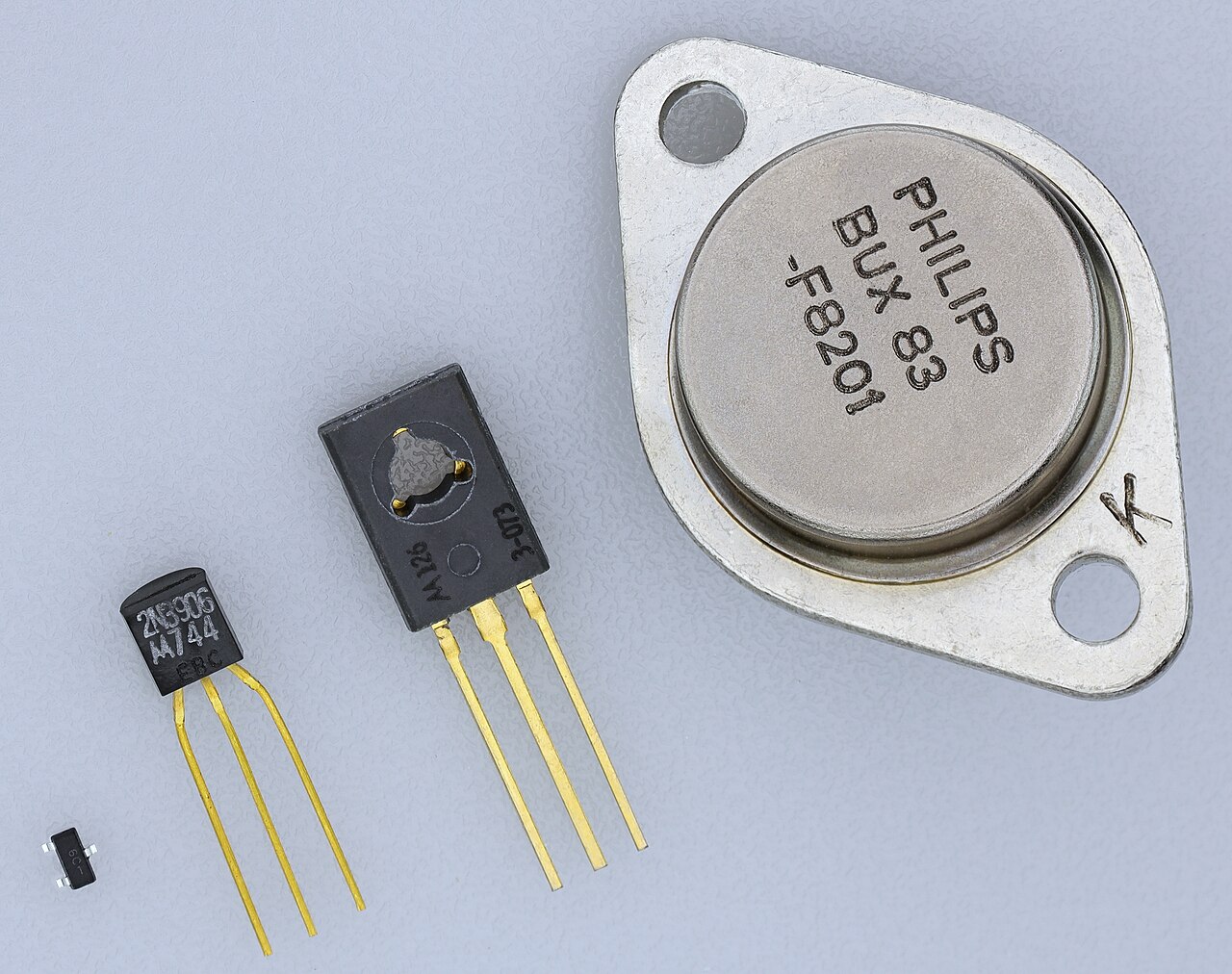
Let’s take the most obvious miniaturisation measure unit: the transistor count. It represents the number of transistors in an electronic device. The first transistor was invented in 1947 by physicists John Bardeen, Walter Brattain, and William Shockley at Bell Labs, which won them a Nobel Prize. This first model was a centimeter long, but the miniaturisation of transistors progressed swiftly. In 1971 it already was 10 µm long, for approximately 2000 transistors per microchip. Today we have nearly reached 50 billion transistors per microchip, for a size of 3 nm.
Smaller components mean at the same time saving space, being more energy-efficient and saving raw material. Miniaturisation is done while increasing power efficiency.
This attraction for miniaturisation has led scientists to conduct researches, until reaching a point where today’s computers can reach a size similar to a grain of rice.
Let’s zoom in on the world of “smart dust”
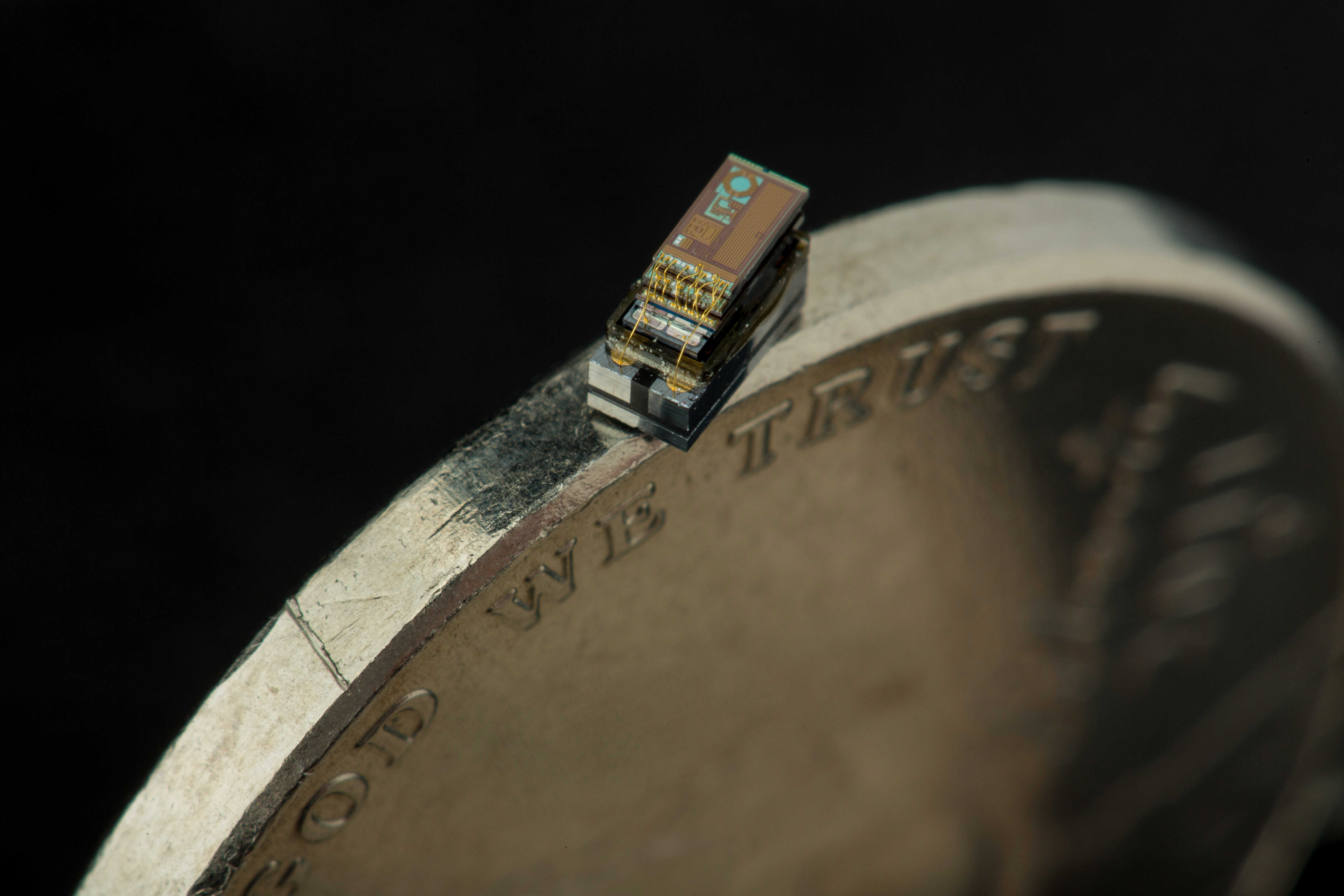
In 2018, the Electrical and Computer Engineering University of Michigan presented its last creation called micro motes. Those extremely small devices, which measure around a cubic millimeter, are the world’s smallest computers. To be exact, they measure on average 2 x 2 x 4 mm$^3$. The main objective of the University of Michigan was to create the smallest autonomous computer. By autonomous I mean that it has to have its own reliable power supply and onboard processor. To do so, they chose to organise their sensors in layers.
The sensors are organised in layers
Each microcomputer of the University’s product line, called M$^3$ sensors, is composed of 8 superimposed layers. Each layer has a specific use.
- Solar cell
- Harvester control electronics layer
- Radio layer
- Sensor interface layer
- Decap layer, stabilising the power supplies
- Processor + memory + power regulation layer
- Battery
- The actual sensor layer
In this model, each layer communicates with the previous one.
This choice of organising the sensors in layers is far from innocuous. Indeed, microsensors can be used in so many different areas. The design of micro motes had to be modular, and easily adaptable for several usages. In addition, as the last layer is the sensor, it is easy to change the type of sensor to obtain the desired device.
Here is a picture of the M3 Imager, along with a diagram representing a cross-section of it:
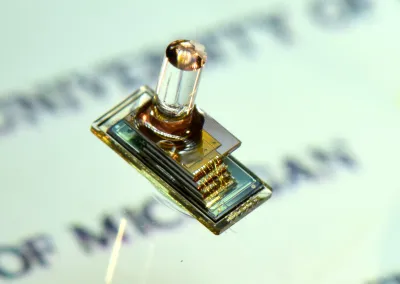
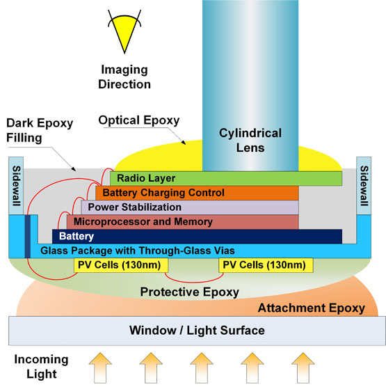
The layers layout is very similar to other M3 devices. Instead of having a cylindrical lens, we could have a pressure or a temperature sensor. Then the microcomputer would only need to be flashed with another program, and it would make another operational micro mote. This step therefore leads to an important question: how to modify or simply flash a program on these microdevices.
How does the micro mote communicate?
It is great to have a small autonomous computer able to gather information, but to be useful it has to transmit some data one way or another at some point. Also, it has to be easily reprogrammable. Two layers are involved in this operation: the solar cell layer and the radio layer.
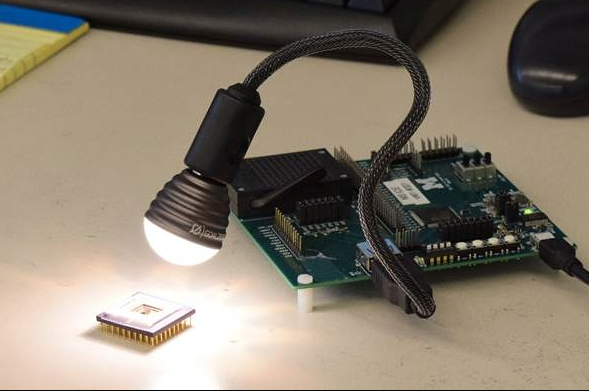
The solar cell layer is used to reprogram the processor. Researchers will flash a light in front of it as a way to transmit the data to write. With this technique, there is no need to connect wires or any physical device to the computer.
The radio layer can transmit the gathered data as far as two meters, thus being a layer that also communicates wirelessly. The radio communication protocol is custom, and tailored to fit micro motes specific energy and storage requirements. Unfortunately, the radio communication protocol is not widely disclosed as it is a proprietary technology developed by the University of Michigan.
How are they so energy efficient?
The energy efficiency is another huge challenge to tackle. The size of the micro mote is an advantage, but also a drawback. The embedded devices are small so they should consume less energy, but it implies having a little battery attached to them too. Thus, power management has to be taken into account.
For this reason, the choice of a specific processor is essential for the computer to work properly. The processor on the 6th layer is a Phoenix processor, which measures 915 x 915 $\mu m^2$. It consumes only 500pW. In comparison, it consumes around 5 x 10$^{11}$ times less power than most commonly used processors for personal computers. It is closer to the energy consumption of a human cell, which is 1pW.
The battery layer is in charge of storing and powering the processor, but it cannot create power. There, is the second use of the solar cell layer. In addition to being the programming interface between the user and the processor, it also harvests solar energy, producing 20nW.
In standby state, the total power consumption of the micro mote is 2nA. Your own smartphone, on standby state, consumes a million times more power than one Michigan’s University devices.
An opening on the future of microsensors
Smart dust is predicted to be useful in many different sectors. It is for example highly profitable for the IoT one, which needs small and energy-efficient components, such as sensors. It can also find usages in biotechnologies and healthcare to monitor patients’ health activities. My guess is that it can be profitable in nearly every field, from agriculture to transportation to the energy sector.
An interesting point is that some of these sectors did not even exist in the early ages of computing. We can then therefore ask ourselves, what is the future of this constant progress of smaller technologies?
The University of Michigan is not the only and the first organisation to work on developing smart dust devices. The company Hitachi, for example, has developed in 2006 “Hitachi mu-chips”, the world’s smallest rfid chip. This version mesures only 0.15 x 0.15 millimeters in size and 7.5 micrometers thick. It is the successor of an older version, a 0.4 x 0.4 millimeters RFID chip also developed by Hitachi 3 years before, in 2003. Although Hitachi chips are currently the most-used micro RFID chips, progress is still made nowadays. In 2021, a Gen-2 compatible RFID chip was introduced during the IEEE International Conference on RFID, which took place at North Carolina State University. That one measures 125μm × 245μm.
For the moment being, Michigan’s micro motes are not able to communicate with each other. They have to be 2 meters away from a base station for the user to be able to retrieve collected data. Establishing ways to communicate between those microcomputers is an essential part of its evolution. It would indeed allow to build a mesh of sensors, each one being able to pass on meaningful information to the next computer, until eventually reaching the end base station. The university’s researchers are currently working on this feature, along with expanding the range of the smart dust up to 20 meters. I consider this step to be crucial for the success of this technology.
Ultimately, miniaturisation, as well as other highly active research sectors, can and surely will lead to the creation of unsuspected technologies and field of application of already existing ones.