Table of Contents
- Introduction
- First approach
- Recovery Mode, Boot and Power Management Processor, how does it all work?
- The Recovery Mode and the abuse of the memory layout
- Conclusion
- References
- Going further
Introduction
Over the years, Nintendo has had numerous issues with the security of its consoles. The SNES had the Super Wild Card, the GameBoy and GameBoy Advanced had flash cartridges, and the DS/3DS and Wii consoles suffered from software-based exploits. In 2016, with the upcoming release of the Nintendo Switch, Nintendo announced being partnered with Nvidia for the console’s SoC: the Nvidia Tegra X11. Like every console before it, a large amount of researchers were interested in seeing if they could find a way to run unverified code on the console, and this is where the story begins.
Prerequisites
To fully appreciate this article, you should have some knowledge of the following topics:
- Some low-level knowledge, more specifically about return pointers,
- Basic C/C++ understanding, in this case, buffer overflow and some I/O operations,
- Basic knowledge of what a SoC and a booting process is,
- Basic knowledge of what a USB device is and how it works.
Disclaimer
This article is not a “how to hack your Switch”. It is only meant as a dive into how researchers figured out an exploit to run unverified code on the Nintendo Switch and was purely written for educational purposes.
First approach
Compared to most of Nintendo’s consoles up to this point, the Tegra X1 SoC had something that most of its previous consoles’ chips did not have: public documentation. Indeed, the Tegra X1’s data sheet2 is available online, making it a prime target for security researchers.
However, the Switch appeared to be a much more secure environment than its predecessors. No hardware backward compatibility with previous consoles, and for emulated games, they were all run on a closed-off sandbox environment. Where the Wii and 3DS were respectively first hacked through their GameCube and DS functionalities, the Switch had nothing of the sort.
Yet, in January of 2018, less than a year after the Switch’s release, this all changed when the hacker group fail0verflow released a video3 showing the first successful “coldboot” exploit on a Nintendo Switch. While they would choose to keep their discovery private for the time being, it all changed a few months later in April, with the first successful unauthenticated arbitrary code execution being shown to the public, this exploit being known as Fusée Gelée4.
To understand all this, one needs to take a look at the Tegra X1 booting process as well as parts of its architecture.

Recovery Mode, Boot and Power Management Processor, how does it all work?
So now, how does one find such oversight? What angle of attack is there, and how to approach it? To figure this out, one needs to take a look at the Tegra X1 booting process as well as parts of its architecture.
When being powered on, the first thing the chip does is go through something called the Boot and Power Management Processor, or BPMP, shown in red in the following diagram.
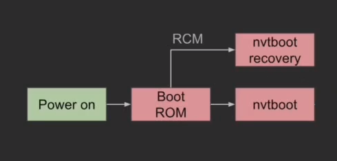
The only part interesting in the scope of this article is the boot ROM, which is the first thing the chip executes, and the recovery mode, which is what the chip enters when it encounters an issue during the booting process or when forced to do so. However, for references, the nvtboot corresponds to “the bootloader code loaded by the boot ROM and executed on the boot CPU”5, which is the last step before the first code execution on the main CPU complex, meaning that it is the last step before the actual booting process.
The BPMP is a processor that is part of the chip responsible for running the code stored in the boot ROM, which consists mostly of security checks.
BPMP and the idea of secure boot
Secure boot is a vital part of any modern embedded firmware whose purpose is to ensure that the code executed by the device during the booting process is verified and trusted.
This is done by checking the integrity of the code executed at each step of the booting process, and the Tegra X1 is no exception to this. This integrity check made at each step is what is called a chain of trust.
Any secure boot procedure starts with a root of trust, which is the first step of the chain of trust. The root of trust is usually a hardware-based component tasked with verifying the integrity of the next step in the chain of trust, and so on until the booting process is complete.
This implies that the boot ROM too is a root of trust, and it is the first step in the chain of trust of the Tegra X1, and ensures that the bootloader is sound and can be executed. The idea of a chain of trust is also not specific to the Tegra X1, and consists of a series of steps that are all verified by the previous step, and the last step of the chain of trust is the actual booting process. In the diagram above, the boot ROM is the root of trust, and the nvtboot is the last step of the chain of trust.
This is why the BPMP is ultimately the only measure preventing anyone from running arbitrary code on the Switch. So, how can it be bypassed?
Exploiting the boot ROM
As mentioned earlier, the boot read-only memory, or boot ROM; is what gets executed first when the console powers up. However, modifying the code executed by the boot ROM is no easy task.
Indeed, every step in the booting process checks, through hashes and signatures, that the integrity of the code run in the next step is sound. It means that changing the code run by any of these steps would only result in said code not being executed, rendering useless all efforts made.
Fortunately, circumventing this is, in theory, fairly straightforward as only the security around the boot ROM needs to be defeated. Since it is the root of trust, defeating that security means being able to run arbitrary code, and this is where all the researchers’ efforts were put towards.
Accessing the Recovery Mode
Like any modern device, whenever an issue arises during the booting procedure, it results in the device booting in recovery mode, and the Switch follows that same pattern. The recovery mode can also be forced, but unfortunately, it also has security measures in place to avoid loading arbitrary code unless the code is signed using a specific private key… that only Nintendo has.
The only viable option here is to come back to the boot ROM to try and find some vulnerability that could be exploited with the recovery mode. This is where the development kit mentioned earlier comes into place. Since the code inside of the boot ROM has no available source online, and no binary can be found either, the only solution is to try to access the boot ROM memory on the development board and directly read it.
A glitch was eventually found, however, forcing the Switch to boot into recovery mode is rather awkward. Every device has a specific combination of buttons to press to force it, the Switch needing the user to press volume down, the Power button, and the Home button.
Except, the Home button is what the Tegra X1 chip calls the “Home” button, which is actually the tenth pin on the Joycon connector, which cannot be accessed easily. This is why people started using a paper clip to short that pin, leaving the user to only need to press power and volume down.

The Recovery Mode and the abuse of the memory layout
When entering the recovery mode, the Switch’s screen stays off and the console works as a USB device. Again, this cannot be used to exploit the boot ROM, as one would need Nintendo’s private key to send a valid message to be executed by the boot ROM. Thus, the idea was to find an exploit that would happen even before any message sent through the recovery mode would be verified.
Sending messages from and to the Switch
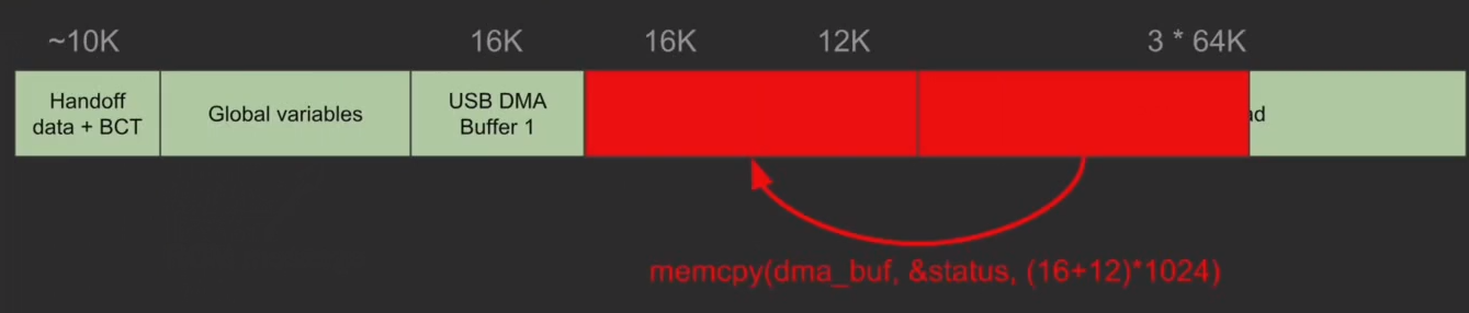
In reality, how messages are sent is not as important as where they are stored. Indeed, the boot ROM is made of continuous physical memory split into different parts.

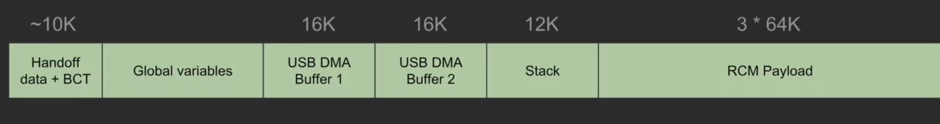
When looking at the layout shown above, three sections should catch one’s eye: the USB DMA Buffers, which will be explained shortly, the stack, and the RCM payload.
The RCM payload’s usage is straightforward: any message sent via USB to the Nintendo Switch is made of two parts; the header and the payload, stored in the RCM payload buffer. Those messages are read asynchronously as bits of data initially stored in the RCM payload are copied by chunks into one of the two DMA buffers.
How the buffer overflow works
Those buffers are used by two endpoints: a control endpoint (EP0) and a bulk endpoint (EP1). This explains why there are two DMA buffers, one for each endpoint as they can be used simultaneously since there could be a call to the control endpoint while data is being sent through the bulk endpoint. The bulk endpoint’s purpose is to send and receive data to or from the console, while the control endpoint supports all the standard USB control transfers, for example: GET_STATUS, which is important for later. Those control transfers have a specific structure, which is as follows:
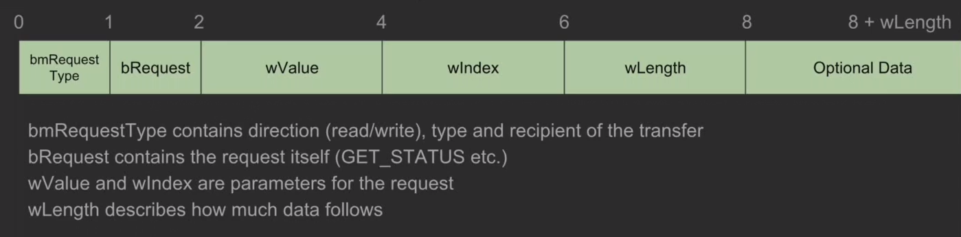
wLength is particularly interesting here, as it is the length of the data to be sent and it is a value that is set by the host, meaning it can be set to any value, including a value larger than the actual data to be sent.
This is where the buffer overflow comes into play.
The handling of the control transfers is done by a function called handle_ep0_control_transfer, which has a particular behaviour for the GET_STATUS transfer.
Indeed, when looking at the following code:
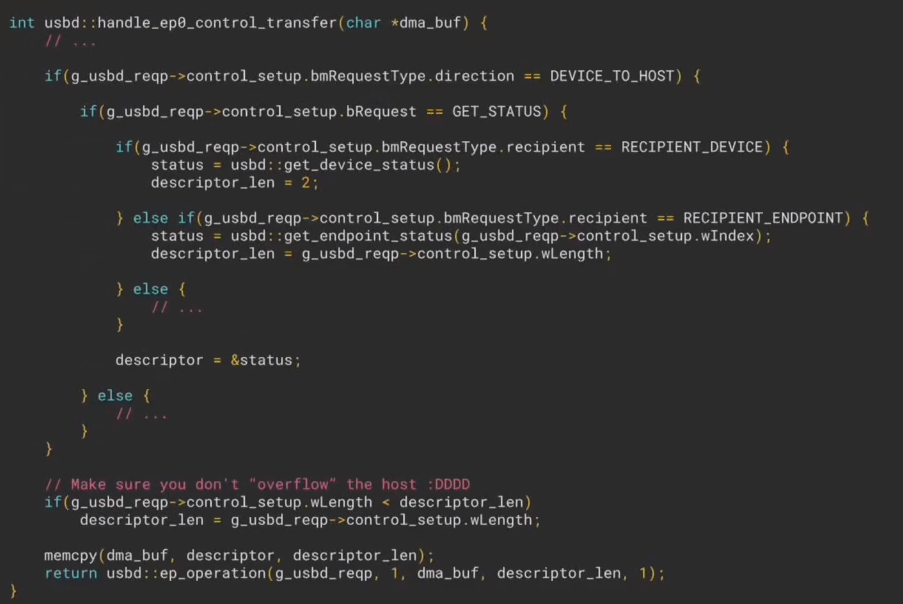
One can notice that in the case where the recipient is equal to RECIPIENT_ENDPOINT, the variable descriptor_len is set to the wLength variable mentioned earlier.
This is important because the status descriptor is 2 bytes long so the memcpy instruction should only copy 2 bytes of data, in theory.
However, the memcpy instruction copies descriptor_len bytes of data, and descriptor_len is set to the value of wLength, which is set by the host.
This means that the host can set the value of wLength to any value, making it possible to overflow the stack as soon as the value of wLength is larger than the 16KB of the DMA buffer and the 12KB of the stack.
Overwriting the return pointer
This is where the return pointer comes into play.
A return pointer is a value stored on the stack that is used to know where to return to after a function call.
In our case, where the stack overflow happens, the return pointer points to handle_ep0_control_transfer as it is the function that called the memcpy instruction.
This implies that it is possible that, instead of returning to handle_ep0_control_transfer, to return to any function whatsoever, including a function that would be stored in the RCM payload buffer, which is where the unverified code sent earlier has been sent to.
Also, since the initial GET_STATUS request stopped the copy of the data from the RCM payload buffer to the DMA buffer, the boot ROM still thinks that the data transfer is not complete, meaning that the signature check is never executed on the code that was sent to the Switch, allowing for arbitrary code execution.
Conclusion
This exploit really shows how even advanced security measures can be bypassed with a bit of creativity. It also shows how important it is to have a good understanding of the hardware one is working with, otherwise, it would have been impossible to find this exploit. Also, the exploit was unpatchable, forcing Nintendo and Nvidia to release a new version of the Tegra X1 chip, the Tegra X1 Mariko, but it still meant that potentially millions of Switches could still run unverified code if their owners wanted to.
This raises the question of how to render a device unexploitable, hopefully assuming that this is even possible. Will there ever be a device that cannot be hacked? Or will there always be a way to bypass the security measures put in place? This is a question that only time will answer.
References
- Nintendo Switch (NVIDIA Tegra X1) - BootROM Vulnerability by LiveOverflow
- Fusee Gelee’s Vulnerability Disclosure
- Embedded secure boot
- Nvidia’s “Understanding Security”
- Root of Trust and Chain of Trust
Going further
-
https://www.nintendolife.com/news/2016/10/nvidia_tegra_officially_confirmed_as_the_tech_behind_nintendo_switch ↩︎
-
https://cdck-file-uploads-global.s3.dualstack.us-west-2.amazonaws.com/nvidia/original/2X/1/1eecf66463f700c4515bfe091b2a0f6527d13571.pdf ↩︎
-
https://github.com/Qyriad/fusee-launcher/blob/master/report/fusee_gelee.md ↩︎
-
https://http.download.nvidia.com/tegra-public-appnotes/t210-nvtboot-flow.html ↩︎