Table of contents
Introduction
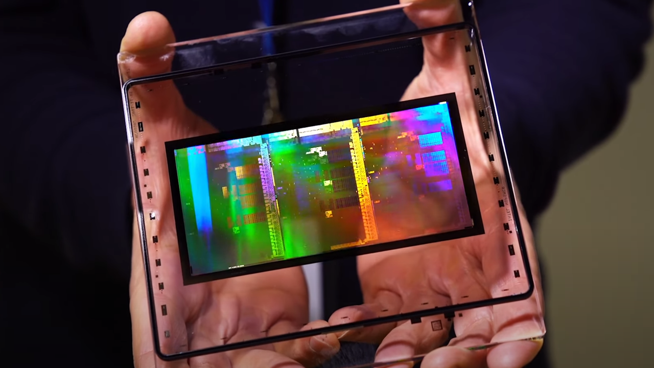
Modern processors, or CPUs, represent the peak of current technology, packed with billions of microscopic transistors. But producing these chips is no easy feat: it involves extremely precise procedures, cleanrooms that are virtually free of dust, and cutting-edge materials like ultra-pure silicon. As tech demands more speed and efficiency, the manufacturing process gets even more complicated. The race to manufacture chips smaller, faster, and more powerful pushes the boundaries of science and engineering, making CPU production one of the most complex processes in the world. Let us dive in the process of manufacturing a CPU from silicon to the chip and then we will discuss what make this process more complex over the years.
How are they manufactured?
Design
In the first place, we need a design: not every chip is developed to be used everywhere and so, we design them in a certain way so there are employed for some tasks. Among the things we can alter during the designing process, we can talk about:
- architecture,
- logic design,
- voltage,
- transistors layout,
- etc.
This design is then used to create a photomask, which is a plate that reflects light in a certain way. This is what a photomask usually looks like:
This is used during the photolithography step to apply a pattern on a silicon wafer, which we will talk about later.
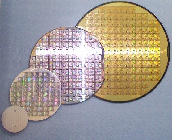
Silicon wafer
Once we prepared the previous steps, we need a surface on which we will work on. In the semiconductor process, we will be using a silicon wafer. It is built with a very purified kind of silicon which has gone through many steps to make it extremely pure (growing, cutting, shaping). It is coated with an oxide layer that will be modified later on by the layers of transistors that we will add on top of it.
From now on, steps will be explained in a certain order to be the most understandable. But it is significant to note that not every chip manufacturer does the same steps at the same time or at the same rate. Sometimes, some steps are even done before others, so keep in mind that steps order is subjective starting from the following point.
Photolithography
We currently have the silicon wafer and the mask. We need to place the mask on the wafer using photolithography. To do so, we first coat the wafer with a photoresist liquid primarily made of resin. Next, we put the photomask on top of the CPU that has been coated, and we project UltraViolet (UV) light through the mask and this process will produce a pattern on the coating.
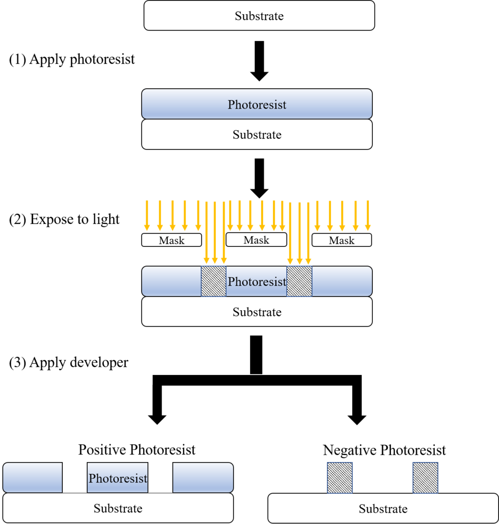
We need to remove the negative photoresist spots where the light has been projected by the mask on the photoresist. To do so, we employ a solution called a ‘developer’. A developer is a chemical solution used to reveal the pattern of the circuit on the wafer by dissolving the negative photoresis.
Once the desired pattern has been revealed on the wafer surface using photolithography, the process moves to etching, where this pattern is permanently transferred into the underlying layers by selectively removing exposed material. But before etching, manufacturers might want to dope the chip.
Doping
Why? Because we need to maintain a precise control of the conductivity of each layer of the wafer. Thanks to this process, we will alter the electrical properties of the silicon by bombarding the wafer with ions through a process called “ion implantation.”
Etching
Currently, we have the photoresist on the wafer, and we need to etch the pattern on the oxide layer below. There are two kinds of etching: wet etching and dry etching. The first one is outdated so we will only approach the second one. Plasma is shot through the photoresist to etch the oxide. Once the process is completed, we can ultimately remove the photoresist layer by employing another solution that will be soluble with it.
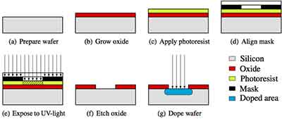
This diagram shows the etching process before the doping one but as we said in the beginning, steps can be done in a distinct order, depending on who builds the semiconductor.
Metallization
To enable communication between transistors, we need to connect them. To do so, the chip undergoes a process called “metallization”, in which tiny wires are placed on the wafer to connect the billion of the transistors on a layer and make them function as a unified processor. This process is overly complicated and involves many steps like:
- Chemical Vapor Deposition (CVD) allows to deposit insulating materials and conductive layers like tungsten or silicon dioxide.
- Atomic Layer Deposition (ALD) is used for surgically precise barrier layers that prevent metal diffusion. Tantalum nitride or titanium nitride are typically used here.
- Physical Vapor Deposition (PVD) represent the key step in which the metal layers themselves are applied on the chip, using copper or aluminium.
Planarization
Once we provide various layers of materials deposited and patterned on the wafer, we need to flatten up the surface. Come in the planarization, which will smoothen the surface. This is achieved because there can be bumps, ridges or any kind of irregularities that appeared during the previous step and to ensure that they do not affect the performance of the wafer, we extract them as much as possible. Planarization can be done multiple times during the manufacturing of a wafer to ensure that each set of layers are as smooth as possible.
Photolithography, etching, doping and metallization are repeated many times (usually a dozen), to make up the whole semiconductors circuit. Once some layers have been done, they are planarized and the process repeats itself until the whole wafer structure is done.
Wafer testing
The wafer is now ready, it needs to be tested to ensure it follows the behaviour that it was designed for. This step is critical to define which wafers are good enough to be put with others wafers.
First, a wafer prober is used to check for integrated circuits thanks to microscopic probes. The machine is made to position each chip accurately under the test probe. Next, an important component comes in: the probe card. This item, made of very tiny needles, will check for electrical problems in the wafer. It will simulate real-world operating conditions, while also checking that the test patterns it has been given are working correctly on the wafer. There are many types of probe cards, and some of them very advanced and must be extremely accurate since the operate on a nanometer scale.
A die can be marked as defect if it has problems like short circuits, faulty transistors or even issues with insulation layers. Even if a card fails some tests, it will not be thrown away but only used in lower-tier products. This is called “chip bining” and we will cover this subject later on.
Once we ensure that a wafer passes all the tests, it can be cut to form what is called a “die”, which is an individual chip that will be part of the final CPU.
Dicing
As we said before, we now have a perfectly working chip but it is still part of the wafer and we want to combine it with other chips to create the final CPU. The wafer goes through dicing, in which it will be cut, so it becomes a die. There are many sub-steps that can be done here, depending on what kind of final product we want. Some of them are:
- Inspection: the wafer is thoroughly inspected for any scratches or cracks, which could affect the performance.
- Coating: in some cases, a thin protective layer of polymers can be applied on top of the wafer to protect it during the dicing process.
- Wafer mounting: The wafer is then mounted on a metal frame using dicing tape, a very specific kind of tape that will be removed once the cutting has be done.
- Back grinding: To reduce the thickness of the die, the wafer is sometimes grinded and polished. This is usually done when chips are manufactured for minimal chips in USB sticks, smartphones, MP4, etc.
When all the preparation has been done, the wafer is cut and the wafer tape is removed to only keep the working die.
Packaging
The final step, packaging, is done when every die is ready to be mounted with other dies. They are first attached on a lead frame with epoxy, that can have many types of shapes depending on what kind of CPU we want at the end.
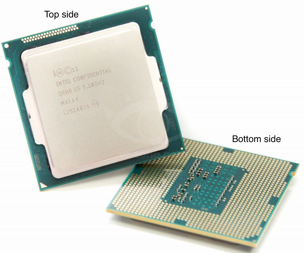
Then we need a package: a case made of plastic, ceramic or metal that will make the board able to connect the device with a circuit board like a motherboard. This is typically what we think about when we speak about CPUs, on which the manufacturer and the type of CPU are written. Here is a typical package that we can see every day:
Next, all wires in all the dies are bonded with think wires of gold, aluminium or even copper. Silver can also be used since it is highly conductive but can corroded very fastly compared to the other materials.
And finally, once all the dies are connected, they are encapsulated in the package and we have it: the CPU!
Final tests are done to ensure the CPU is working as expected before being shipped for selling. This testing is called yield, and information about it is quite hard to get since manufacturers do not often communicate it.
Now that we have explored the intricate steps involved in manufacturing CPUs, it is clear that producing these chips demands incredible precision and cutting-edge technology at every stage. However, as these processors become smaller and more powerful, the challenges in maintaining efficiency and reliability have grown significantly. So why has the process become so complex over the years? Let us dive into the key reasons behind these increasing challenges in modern chip manufacturing.
Why is it this complex?
Cleanliness
As you may have seen, the process is extremely complex and needs high-precision machines to be done. Those machines are also very sensitive to pollution like dirt since we only operate with incredibly high-quality materials. For example, the silicon has “a purity of 99.9999999% (9N) or higher” and we would like to keep it that pure. To do so, the factories are extremely clean to the point that they are classified as Class 10 and Class 100 clean room facilities by Cleanroom. A Class 10 cleanroom has no more than 10 particles larger than 0.5 microns per cubic foot, preventing contamination during sensitive processes like photolithography and etching. It can go to 100 particles larger than 0.5 microns per cubic foot for Class 100, which is a bit less strict for less sensitive steps (you can find more information about it here).
Also, human interaction with those machines is very restricted: since they are extremely precise (and also very, very expensive), we need to be sure that we do not contaminate any part of the manufacturing process. Scientists wear Personal Protective Equipment (PPE) and ElectroStatic Discharge (ESD) shoes to prevent any damage on the components. Some steps of the manufacturing process are performed by humans, such as carrying the wafers from a machine to another one, but they are minimal as human beings are the most susceptible to damage any part of the CPU.
Techonology evolution
The manufacturing is highly precise: These chips are as small as a nail and can compute 17 trillion operations per second. One of the most challenging part about it is the size of a transistor: we currently are at a minimal size of 3 nm and we are about to hit the 2 nm mark in 2025. We are also expecting the 1 nm mark around 2027. The manufacturing process evolves years after years and what I have explained in this article might be outdated in 5 or 10 years.
CPU evolution will slow down due to physical limitations and the challenges of continued miniaturization and the reason to this is called the Rayleigh criterion: to brief it, there is a Critical Dimension (CD) that is the minimal size we can print transistors on a wafer using photolithography. It depends on three factors:
- the wavelength of the light we use,
- the Numerical Aperture (NA) which is, to make it simple, the amount of information the lens we use can collect,
- and the k1 factor is a “coefficient that depends on many factors related to the chip manufacturing process”.
Scientists say that we are certainly coming to a time where we will hit the limit of this formula, and we will not be able to print smaller transistors on wafers, which is currently one of the biggest upgrades in each generation of CPUs.
There also is a problem because of the Moore’s Law: it indicates that the number of transistors in a chip should double every two years. Computers are revolving around the law and manufacturers have been able to keep up with it for the last 30 years, but there is currently a concern about continuing this way because it depends on the evolution of technologies. The doubling time might be extended to three years instead of two according to Intel’s CEO, Pat Gelsinger: it will not die yet and Intel will keep up with the law. AMD’s CTO said the opposite, that we enter the ‘Era of a Slowed Moore’s Law and the conflict is currently on. Nobody is sure about the future of CPU manufacturing and we might be spectating a big revolution in the next years.
An alternative that is being studied are graphene and carbon nanotubes, because they offer many properties that could be very important in the future like heat conduction, transparency and even a high electron mobility. This article details about the process and how a group of engineers from MIT built a chip made of carbon nanotubes.
Environmental impact
A very modern problem that has also been seen in semiconductor manufacturing: it creates a lot of pollution.
First, like you saw in the previous part, we use many, many machines to build one CPU. Those machines consume a high quantity of electricity: 100 megawatt-hours in the large chip plants and TSMC used 5% of Taiwan’s electricity in 2019.
There is a huge consumption of water: TSMC used 63 million tons of water in 2019 and this Forbes article says that a chip factory uses 1 million gallons of water daily which is equivalent to 3,785,412 liters per day.
Another debate is around the pollution produced by those factories, Intel’s campus in Arizona produced 16,078 short tons of waste and 291,805 MtCO2eq of greenhouse gases. This is common to all CPU factories to produce this much waste and to pollute the air.
Manufacturers are currently changing their manner of producing as we can see on Intel’s website.
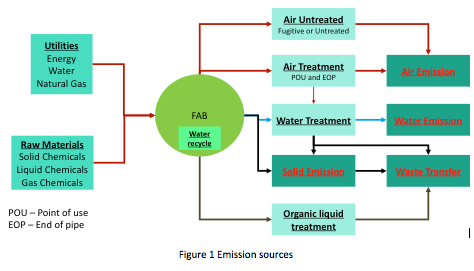
This image from semiconductor-digest.com summarizes perfectly this issue:
Cost
Producing a CPU is extremely expensive. Intel spent over 3 million dollars in 2021 in research and development of their 4nm technology. And even the price of the factories themselves is ridiculously high: Samsung said their new plant in Texas costs 25 billion dollars dollars. Intel also wanted to open a new factory in Germany that would have cost 18.7 billion dollars but because of the inflation and the price of materials that has risen, it is currently estimated at 31.675 billion dollars. Those prices are very alarming and will not be going down in the current state of economy: “The higher construction cost is about 80% of the cost increase”.
Heat
Since transistors are becoming smaller over the years, there is a huge problem about heat in the CPU. This article is extremely precise and I highly encourage you to read it. Here is a summary of the bullet points mentionned in the article:
- CPUs experience short bursts of high power consumption, which can be up to six times the steady-state level. These bursts increase temperature rapidly but are managed through advanced power delivery systems that prevent excessive heat buildup.
- Modern CPUs, especially multi-core processors, exhibit a highly dynamic power profile. Power consumption varies based on the workload, and thermal management is designed to handle these fluctuations. The system manages power density, ensuring that “hot spots” on the chip do not exceed allowable limits.
- CPUs are designed to maintain a steady junction temperature, which is the temperature inside the silicon chip. Even under maximum load, the CPU manages this temperature to ensure reliability and longevity. However, occasional bursts of high performance do push the junction temperature higher temporarily.
- The article presents tests of different workloads, including human interactive tasks and benchmarks like SPEC and 3DMark. The results show that CPUs can take advantage of thermal headroom to temporarily boost performance, but this comes at the cost of heat, which must be managed carefully.
- In systems with multiple processing components, like CPUs with integrated graphics, power budgeting is critical. The system dynamically allocates power between the CPU and other components to balance performance and thermal limits.
Conclusion
The production of processors has become increasingly complex due to several factors that drive advancements in semiconductor technology. Modern CPUs are built from billions of microscopic transistors, using sophisticated techniques. These processes demand incredibly pure materials, ultra-precise equipment, and take place in highly controlled cleanroom environments.
As transistor sizes shrink to nanometer scales, thermal management, power efficiency, and manufacturing costs have become critical concerns. The quest for better performance and power efficiency is pushing engineers to explore new materials and architectures, adding layers of complexity. As a result, the production costs of fabs have soared into the tens of billions, while technological challenges, such as managing heat and maintaining reliability, grow more difficult with each new generation of chips.
To conclude, the intricate demands of modern processor manufacturing stem from the pursuit of ever-smaller, faster, and more power-efficient chips, making it one of the most complex processes in modern technology.
Bibliography
- https://www.youtube.com/watch?v=jx-w2o-Lj8g
- https://www.electronicsforu.com/special/demystified-cpu-manufacturing-process-technology
- https://en.wikipedia.org/wiki/Semiconductor_device_fabrication#List_of_steps
- https://oricus-semicon.com/what-is-the-die-attach-process/
- https://www.youtube.com/watch?v=SrckOCFGBrs
- https://www.bit-tech.net/reviews/tech/cpus/how-to-make-a-cpu-from-sand-to-shelf/1/
- https://www.pureairsystems.com/2022/05/09/hepa-systems-for-new-intel-chip-manufacturing-facilities/
- https://hourglass-intl.com/understanding-cleanroom-glove-classifications/
- https://en.wikipedia.org/wiki/Wafer_(electronics)#Formation
- https://hourglass-intl.com/understanding-cleanroom-glove-classifications/
- https://www.asml.com/en/news/stories/2021/semiconductor-manufacturing-process-steps
- https://en.wikipedia.org/wiki/3_nm_process
- https://www.asml.com/en/technology/lithography-principles/rayleigh-criterion
- https://insidetelecom.com/what-reaching-the-size-limit-of-the-transistor-means-for-the-future/
- https://www.tomshardware.com/tech-industry/semiconductors/intels-ceo-says-moores-law-is-slowing-to-a-three-year-cadence-but-its-not-dead-yet
- https://www.tomshardware.com/news/amd-cto-mark-papermaster-more-cores-coming-in-the-era-of-a-slowed-moores-law
- https://medium.com/@rahulsaha.juetce/graphene-processors-and-the-rise-of-carbon-nanotubes-6b92e080e511
- https://www.theguardian.com/environment/2021/sep/18/semiconductor-silicon-chips-carbon-footprint-climate
- https://fortune.com/2024/01/29/chips-act-semiconductor-factories-environmental-impact-water-electricity-carbon-chemical-waste/
- https://www.exploreintel.com/ocotillo
- https://www.intel.fr/content/www/fr/fr/environment/intel-and-the-environment.html
- https://www.semiconductor-digest.com/sustainability-in-semiconductor-manufacturing-a-review-of-emissions-and-materials-released-off-site/
- https://hardwaretimes.com/intel-7nm-cpu-production-costs-down-by-30-rd-spendings-on-4nm-up-by-1-6-billion/
- https://www.anandtech.com/show/18774/inflation-rises-fab-costs-for-intel-and-samsung-by-billions-of-dollars
- https://webee.technion.ac.il/people/ran/papers/Therminic2013_efraim_rotem_2013.pdf